
Circuit Diagram
Index 580
74 Series digital circuit of 74142 BCD counter / 4-bit latch / BCD decoder / driver
Published:2011/7/25 3:14:00 Author:Lucas | Keyword: 74 Series, digital circuit , BCD counter, 4-bit latch, BCD decoder, BCD driver

All other outputs are off.
It contains a BCD counter, a 4-bit latch and a decoder, Nixie tube driver; the counter accepts input clock frequency which is up to 20MHZ; driver tube has the same input with 74141.
(View)
View full Circuit Diagram | Comments | Reading(3276)
74 Series digital circuit of 74141 BCD decimal decoder / driver
Published:2011/7/25 3:14:00 Author:Lucas | Keyword: 74 Series , digital circuit , BCD decimal decoder, BCD decimal driver

It can drive inflated cold-cathode display tube directly; all decoding input could ensure that all outputs of invalid code are off; the maximum reverse current of NPN output transistor is 50mA whenunder 55V.
(View)
View full Circuit Diagram | Comments | Reading(1811)
Power drive circuit with 180°output phase differencebetween normal and opposite phase
Published:2011/7/25 3:08:00 Author:Lucas | Keyword: Power drive circuit , 180°, output phase difference , normal , opposite phase


If the common emitter current of VTl and the two transistors in the first differential amplifier circuit composed of A2 chip are equal, then the following equation is effective, Av2 is the open-loop gain of A2. If the open-loop gain of A1 is AV1, then the positive phase output U01, feedback factor, input voltage can be gotten by the following equations. Comparing with the equations (2-2) and (2-3), if A (V1) = A (V2), the U. 1/Ui and U. 2/Ui have the same frequency characters. For any frequency, the normal-phase output U. l and the inverted output U. 2 have 180 °phase difference.
(View)
View full Circuit Diagram | Comments | Reading(749)
The centralized controller of drainage and irrigation pumping station Two
Published:2011/8/8 21:43:00 Author:Felicity | Keyword: centralized controller, drainage and irrigation pumping station

First turn Q on, and press S2 in the control room or S1 in the irrigation and drainage machine room. Then the phase voltage of L1 goes through the normally open contact of S2, signal line a, normally close contact KM2b, KM3b, KA3, KT, AKA2 to null line to make up current circuit. And KT turns on and KM1, KM2 closes in succession and the pump motor starts as Y step-down start. When it need to stop , pressing S2 or S1 again to make KA turn on, the normally open contact of KA1 close ,then the normally open contact KA2 and M3 turns off to make KM2 and KM3 release and the pump motor stops. (View)
View full Circuit Diagram | Comments | Reading(687)
The Circuit Diagram of Q-adjustable Band-stop Filter (741)
Published:2011/8/8 21:43:00 Author:Felicity | Keyword: Band-stop Filter , Q-adjustable

The notch frequency and the stability of Q depend on the passive components in the T-network. Appropriate components can make up a stable filter in this way. To build up a notch filter of high stability, passive components of high precision is needed besides high-performance operational amplifier. If R and C have the opposite temperature coefficient and R1, R have the same temperature coefficient, ω0 and Q are stable. (View)
View full Circuit Diagram | Comments | Reading(1926)
74 Series digital circuit of 74LS326 dual VCO(two-way output with controlling)
Published:2011/8/9 3:29:00 Author:Lucas | Keyword: 74 Series , digital circuit , dual VCO, two-way output, controlling


There are two independent voltage-controlled oscillators; output frequency is determined by the external components; it can works at any frequency between 0.12Hz and 30MHZ; it has the complementary output and allowable input end.
(View)
View full Circuit Diagram | Comments | Reading(1174)
74 Series digital circuit of 74LS321 crystal-controlled oscillator
Published:2011/8/1 20:51:00 Author:Lucas | Keyword: 74 Series, digital circuit, crystal-controlled oscillator


It is similar to 74LS320, but there are two TTL-level outputs by counting F / 2 and F / 4.
(View)
View full Circuit Diagram | Comments | Reading(1083)
74 Series digital circuit of 74LS320 crystal-controlled oscillator
Published:2011/8/1 20:51:00 Author:Lucas | Keyword: 74 Series , digital circuit, crystal-controlled oscillator


The working frequency range of crystal-controlled oscillator/ clock pulse is 1Hz ~ 20MHz; TTL level and high level(5V-12V) have 2-phase output.
(View)
View full Circuit Diagram | Comments | Reading(990)
The circuit diagram of 8 order low-pass filter (MAX291,TA7504P)
Published:2011/8/8 21:46:00 Author:Felicity | Keyword: 8 order, low-pass filter

8 order low-pass filter circuit is shown in the figure. This circuit is 8 order low-pass filter circuit adopting switched-capacitor. Changing the clock frequency can change the cutoff frequency and the cutoff frequency is 1/100 of the clock frequency. +5V voltage square wave signal is put on the input terminal of the clock and then between input (IN) and output (OUT) terminal of A1 would get the performance of low-pass filter. Because of the input attenuator and the output amplifier, the input and output signal voltage can be ±10V.
(View)
View full Circuit Diagram | Comments | Reading(1347)
The Circuit Diagram of Text-display Logic-pen Consists of Gate Circuit (CD406) 3rd
Published:2011/8/8 21:46:00 Author:Felicity | Keyword: Text-display, Logic-pen
The circuitof text-display logic-pen consists of gate circuit (CD406) 3rd is shown in this figure (View)
View full Circuit Diagram | Comments | Reading(862)
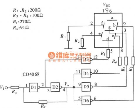
The Circuit Diagram of Text-display Logic-pen Consists of Gate Circuit (CD4011) 2nd
Published:2011/8/8 21:47:00 Author:Felicity | Keyword: Text-display, Logic-pen
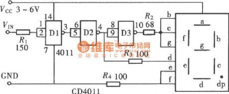
Text-display logic-pen consists of gate circuit has several forms. It can be consist of inverters or NOT-AND gates or NOR gates.The logic-pen shown in this figure consists of NOT-AND gate CD4011 and common anode nixie tube.
(View)
View full Circuit Diagram | Comments | Reading(1508)
The Circuit Diagram of Text-display Logic-pen Consists of Gate Circuit (CD4069) 1st
Published:2011/8/8 21:47:00 Author:Felicity | Keyword: Text-display, Logic-pen
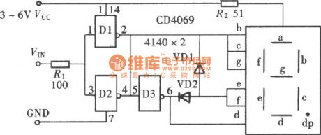
The figure shows the Circuit Diagram of the text-display logic-pen. The text here does not refer to “gao” and “di” in Chinese. It’s H and L, initial letters of High and Low. And it’s easy to use LED to comprise this pen, beacause the shape of this two letters corresponds to the LED circuit. (View)
View full Circuit Diagram | Comments | Reading(778)
The circuit diagram of a logic-pen that can shows the open state 2nd
Published:2011/8/8 21:47:00 Author:Felicity | Keyword: logic-pen, open state
The circuit diagram of a logic-pen that can shows the open state 2nd is shown above. (View)
View full Circuit Diagram | Comments | Reading(446)
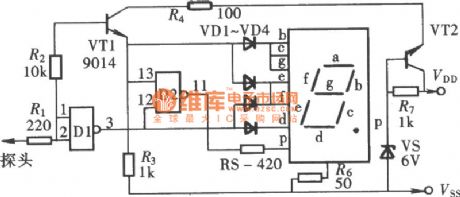
The circuit diagram of a logic-pen that can shows the open state (CD4001) 1st
Published:2011/8/8 21:43:00 Author:Felicity | Keyword: logic-pen, open state
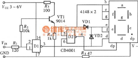
This figure shows a logic-pen that can tests and shows high level, low level and open state of the circuit.
(View)
View full Circuit Diagram | Comments | Reading(762)
OPA2604 Constituted Third Order Low-pass Filter Circuit
Published:2011/8/6 8:46:00 Author:Felicity | Keyword: Third Order, Low-pass Filter

The circuit is showed in the piture above. The circuit makes use of a JFET-inputhigh-fidelityoperational amplifierOPA604 and a dualop ampOPA2604componentthird orderButterworthlow-pass filter. The parameter is showed in the picture. The cutoff frequency of-3dB is 40 KHz. (View)
View full Circuit Diagram | Comments | Reading(719)
The circuit diagram of fourth-order Butterworth 10Hz low-pass filter consists of OPA2111
Published:2011/8/8 21:42:00 Author:Felicity | Keyword: fourth-order, Butterworth, low-pass filter

(View)
View full Circuit Diagram | Comments | Reading(1426)
Logic Pen-based Text Display Formed With The Gate Circuit The 3rd (CD4069) Circuit
Published:2011/8/6 8:46:00 Author:Felicity | Keyword: Logic Pen-based Text Display, The Gate Circuit

View full Circuit Diagram | Comments | Reading(1268)
The Circuit Diagram of Hepatitis Virus Sterilizer Controller Consists of 555
Published:2011/8/8 21:48:00 Author:Felicity | Keyword: Hepatitis Virus Sterilizer

As button AN pressed, the potential transformer B is on and 555 is set because pin 2 is low. And the high voltage output by pin 3 makes contact J1-1 of relay J close and the power voltage is self-hold. Then C1 is charged through W1, R1 and while the voltage reaches 2/3 VDD, 555 reset, and the Contact J1-1 of Relay J releases because the low voltage output by pin 3. And the power is off. And the delay time ,td=1.1(Rw1+R1) C1 ,of 555 is the sterilizing time, which can be adjusted by adjusting W1. (View)
View full Circuit Diagram | Comments | Reading(767)
The Circuit Diagram of 60Hz Notch Filter Consist of INA110
Published:2011/8/8 21:42:00 Author:Felicity | Keyword: Notch Filter, 60Hz

The figure shows the 60Hz notch filter consist of INA110 and double-T network. The 2kΩ potentiometer can adjust Q in this circuit. When the frequency of the city electricity is 50Hz, the resistance of this filter need to be changed, 5.34MΩ into 6.37MΩ and2.67MΩ into 3.16MΩ.This circuit can filter out the AC noise from the circuit. (View)
View full Circuit Diagram | Comments | Reading(1664)
McIntosh Power Amplifier MC-275 Circuit
Published:2011/8/6 8:47:00 Author:Felicity | Keyword: McIntosh, Power Amplifier
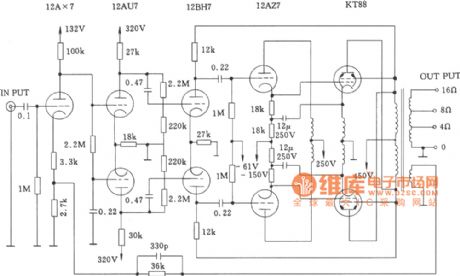
View full Circuit Diagram | Comments | Reading(5336)
| Pages:580/2234 At 20561562563564565566567568569570571572573574575576577578579580Under 20 |
Circuit Categories
power supply circuit
Amplifier Circuit
Basic Circuit
LED and Light Circuit
Sensor Circuit
Signal Processing
Electrical Equipment Circuit
Control Circuit
Remote Control Circuit
A/D-D/A Converter Circuit
Audio Circuit
Measuring and Test Circuit
Communication Circuit
Computer-Related Circuit
555 Circuit
Automotive Circuit
Repairing Circuit