
Circuit Diagram
Index 567
Incandescent life extension device 2
Published:2011/8/10 3:55:00 Author:Ecco | Keyword: Incandescent, life extension device

The incandescent life extension device circuit is composed of the filament preheating circuit, power supply circuit and delay control circuit, and it is shown in Figure 3-198. Filament preheating circuit consists of diode VDl, current limiting resistor Rl and incandescent EL. Power supply circuit is composed of the light switch, step-down circuit capacitor Cl, bridge rectifier UR, filter capacitor C2, resistor R2 and discharge regulator diode VS. Rl and R2 select the 1/2W metal film resistors. RP uses the small solid potentiometer or variable resistor. VDl selects the 1N4007 silicon rectifier diode; VD2 and VD3 choose the 1N4148 silicon switch diodes.
(View)
View full Circuit Diagram | Comments | Reading(584)
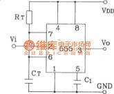
Direct self-excited feedback astable multivibrator circuit composed of 555
Published:2011/8/15 22:23:00 Author:Ecco | Keyword: Direct self-excited feedback, astable multivibrator , 555

View full Circuit Diagram | Comments | Reading(630)
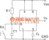
Two kinds of bistable circuits composed of 555
Published:2011/8/15 2:10:00 Author:Ecco | Keyword: bistable circuit, 555


General forms of the bistable circuit composed of 555: RS bistable flip-flop bistable circuit and the Schmitt trigger circuit.
(View)
View full Circuit Diagram | Comments | Reading(891)
Two kinds of monostabtle circuits composed of 555
Published:2011/8/15 22:16:00 Author:Ecco | Keyword: monostabtle circuit , 555
The general monostabtle circuits has two kinds: manual start and pulse-activated.
(View)
View full Circuit Diagram | Comments | Reading(839)
Differential amplifier circuit diagram with 20MHZ bandwidth
Published:2011/8/11 22:30:00 Author:Ecco | Keyword: Differential amplifier, 20MHZ bandwidth
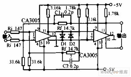
The circuit consists of two CA3005 RF amplifiers, the gain is decided by the ratio Rr / Ri. Capacitors C1, C2 are used to improve the bandwidth to prevent high-frequency self-excitation. Error of resistors is 1%, and the bandwidth is 200MHz, and time delay is 20μs.
(View)
View full Circuit Diagram | Comments | Reading(822)
Voltage-controlled gain amplifier circuit diagram
Published:2011/8/11 22:33:00 Author:Ecco | Keyword: Voltage-controlled, gain amplifier
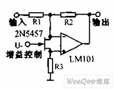
1.53 voltage-controlled gain amplifier is connected to the FET input op amp between the two input ends, and it is used as a voltage-controlled resistor, the resistance changes linearly with the voltage, and the changing range is ten times square, and it has excellent control characteristics. The resistance depends on the op amp.
(View)
View full Circuit Diagram | Comments | Reading(880)
UM95088 Telephone Circuit Diagram
Published:2011/8/9 18:30:00 Author:Vicky | Keyword: Telephone Circuit

UM95088 telephone circuit diagram is shown in the above picture. UM95088 is specialized integrated module of dual tone multiple frequency for telephone dialing. It adopts the techniques of CMOS with dual-in-line package of 14 pins. Dual tone multiple frequency telephone schematic circuit made of the above IC, mainly comprises power supply, key board, dialing and transmitting network, and ad-dc coupling circuit (the ring circuit is omitted in the picture) etc. (View)
View full Circuit Diagram | Comments | Reading(10360)
Circuit diagram of memorial anti-toll-fraud alarm
Published:2011/8/9 20:47:00 Author:Vicky | Keyword: memorial anti-toll-fraud alarm

Memorial anti-toll-fraud alarm
Despite the functions of general anti-toll-fraud telephone, the telephone anti-toll-fraud alarm has functions of alarm for toll fraud by doubling the line, and alarm for toll fraud by breaking the line. In addition, it does not need external power supply. The telephone anti-toll-fraud alarm is mainly composed by CMOS integrated circuit. The composition is very simple. It is mainly polarity reversing circuit (Q1 and Q2), voltage detection circuit (R2, VD1 and VD2), logic-judging circuit (A1), memory display circuit (A2 and V1), and alarm-driving circuit (V2 and V3 buzzer) etc. (View)
View full Circuit Diagram | Comments | Reading(1033)
Automatic Ni-Cd Battery Charger Circuit Diagram
Published:2011/8/9 21:28:00 Author:Vicky | Keyword: Automatic Ni-Cd Battery Charger

Automatic Ni-Cd Battery Charger circuit is shown in the above picture. The internal comparator of NE555 is set as 4.7V by Zener diode. If the potential of pin 6 becomes higher than this value, the output of pin 3 become lower; if the potential of pin 2 is lower than half of the reference voltage, the output voltage becomes higher,. When the voltage of the under-charging battery is very low, the output potential of the IC is high, the battery is charged via R6 and D2 until it’s full-charged. The voltage is set by P2, the state of output of IC is then changed, and the charging process stops. But IC still control the battery temporarily via T1. When the battery output reduces to the level set by P2 due to self-discharging, IC restart charging. (View)
View full Circuit Diagram | Comments | Reading(6765)
C7428 Power Supply Circuit Diagram
Published:2011/7/16 9:12:00 Author:Vicky | Keyword: Power Supply Circuit

View full Circuit Diagram | Comments | Reading(871)
C7458 Power Supply Circuit Diagram
Published:2011/7/16 9:14:00 Author:Vicky | Keyword: Power Supply Circuit

View full Circuit Diagram | Comments | Reading(826)
Hitachi AIPM8C Power Supply Circuit Diagram
Published:2011/7/16 9:17:00 Author:Vicky | Keyword: Hitachi, Power Supply Circuit

View full Circuit Diagram | Comments | Reading(768)
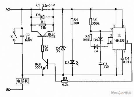
On-Hook Anti Toll Fraud Device Circuit Diagram
Published:2011/8/9 18:26:00 Author:Vicky | Keyword: On-Hook, Anti Toll Fraud

On-Hook Anti-Toll-Fraud Device
The circuit controls the on-off of relay by making use of the changes of voltage brought by on-hook and off-hook of the telephone. S is a exterior switch, which is closed usually. Usually the high voltage of the external line can guarantee the regular work of V (the current of collector is 4mA). The relay works, and the closed contact of K is open, which does not affect the usage of the telephone. When there is toll fraud in the external line, the voltage of the line is lower than 8V, K does not work, and the closed contact makes the external telephone T and R under short circuit. Therefore the external telephone T and R cannot work then. The user can open S, and close it after VD3 is lighted. Then the circuit is under anti-toll-fraud situation. (View)
View full Circuit Diagram | Comments | Reading(1383)
Adjustable voltage-stabilizing voltage circuit diagram
Published:2011/8/9 18:29:00 Author:Vicky | Keyword: Adjustable voltage-stabilizing voltage
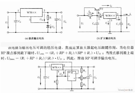
The circuit is a adjustable voltage-stabilizing circuit of the output voltage. Integrated operational amplifier works as voltage follower. When the potentiometer RP slides to the lowest end, U1min = (R1+RP+R2)/ (RP+R1) ·U23;when it slides to the top end, U1max = (R1+RP+R2/R1· U23.
Therefore, the output voltage can be adjusted by sliding the RP. (View)
View full Circuit Diagram | Comments | Reading(604)
Telephone on-hook warning circuit diagram
Published:2011/8/9 18:31:00 Author:Vicky | Keyword: Telephone on-hook warning circuit
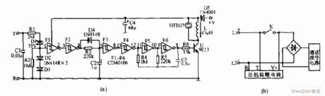
Telephone on-hook warning circuit diagram is shown in the above picture. The IC uses CMOS Shmidt hex inverter CD40106. C1 is better to use ceramic capacitance which can withstand voltage of over 100V, and L is better to choose small color-code inductor. There are no special requirements for the rest component. When the telephone is on-hook, there are several tens of volt-ampere in ends T and R. A short period of sound indicating on-hook is given out via HTD. It is shown in the picture (a). Because the sound only uses the memory function of C4, C4 can only be re-charged when the telephone is off-hook next time after the sound is given out. And the warning sound can be given out when the telephone is on-hook next time. The assembling diagram is shown in the picture (b).
(View)
View full Circuit Diagram | Comments | Reading(1964)
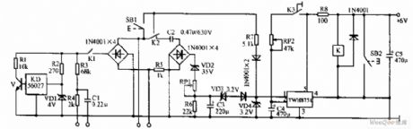
Simple telephone time lock circuit diagram
Published:2011/8/9 18:33:00 Author:Vicky | Keyword: Simple telephone time lock circuit
Simple telephone time lock circuit is shown in the above picture. In the circuit diagram, BG1 and BG2 are electronic switches controlled by IC NE555. When the telephone is on-hook, the DC resistance value of the telephone is over 600KΩ, the current when the external line runs into the IC is very low, and the electronic time lock does not work. When the telephone is off-hook, the telephone DC resistance value reduces to 500Ω, and the electronic time lock works. After the call has been made for a certain period of time, pin 3 of the IC turns into low potential, which forces BG1 to stop. The exterior pressure drop is mainly on the electronic switch, which results in the telephone’s inability to work. And the call is suspended. (View)
View full Circuit Diagram | Comments | Reading(2506)
Telephone Automatic Answering Device Circuit Diagram
Published:2011/8/9 18:34:00 Author:Vicky | Keyword: Telephone, Automatic Answering Device
Telephone automatic answering device circuit is shown in the above picture. The recording telephone device has strong ability of anti-disturbance, which avoids some unexpected matters. When the telephone rings for 6 times without answering, the device will imitate automatic off-hook. Then the telephone is on and gives out the following words: “hello, the host is not in home. Please leave a short message.” Meanwhile, the recorder is connected, and records the detailed content of the speaker’s words. (View)
View full Circuit Diagram | Comments | Reading(2961)
Telephone Automatic Recording Control Device Circuit Diagram
Published:2011/8/9 18:35:00 Author:Vicky | Keyword: Telephone, Automatic Recording Control Device
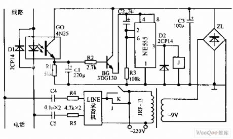
The telephone automatic recording control device circuit is shown in the above picture. When there is ringing signal in the line (90V, 15Hz) or the telephone is off-hook, the delayed pin 3 of NE555 shows high potential, which makes J conducted. The AC power supply of the recorder is conducted by the contact and automatically records the message. It stops recording when the telephone is off-hook or the power supply is cut. K is the manual-operational switch, and is used to control the power supply during sound reproduction. (View)
View full Circuit Diagram | Comments | Reading(1788)
Real-time Telephone Automatic Recording Device Circuit Diagram
Published:2011/8/9 18:38:00 Author:Vicky | Keyword: Real-time Telephone Automatic Recording Device
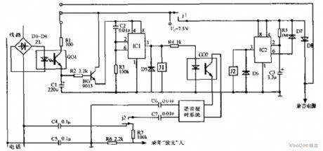
Real-time telephone automatic recording device circuit is shown in the above picture. Despite automatic recording for the making calls and answering calls, the recording device can also automatically input the time of recording before recording the message , which makes the recording material more detailed and accurate and thus easy to be picked out and analysis. IC1 and IC2 in the picture are time-base integrated circuit NE555. The voice timing system uses UT-6657 type made-up timing table. Relay J1 and J2 are HG4098. The coupling device is 4N15, and the diodes are IN4007. (View)
View full Circuit Diagram | Comments | Reading(1823)
Microcomputer Telephone Cost-Saving Device Circuit Diagram
Published:2011/8/9 18:40:00 Author:Vicky | Keyword: Microcomputer Telephone Cost-Saving Device
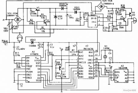
The microcomputer telephone cost-saving device circuit is shown in the above picture. The circuit is made of anti-wiretapping and central processing. PIC16C56 is the central part of the whole circuit. Anti-wiretapping part is composed by VD5-VD8, A4, V4, V5 and HA. The operation of the device is very simple. It has no limitation on the business phones and the phones can be dialed directly; when making business calls, dial the general code first and then dial the telephone number. Then hang up the phone for 4S. The device automatically goes back to the state of limiting the non-business telephone. (View)
View full Circuit Diagram | Comments | Reading(2435)
| Pages:567/2234 At 20561562563564565566567568569570571572573574575576577578579580Under 20 |
Circuit Categories
power supply circuit
Amplifier Circuit
Basic Circuit
LED and Light Circuit
Sensor Circuit
Signal Processing
Electrical Equipment Circuit
Control Circuit
Remote Control Circuit
A/D-D/A Converter Circuit
Audio Circuit
Measuring and Test Circuit
Communication Circuit
Computer-Related Circuit
555 Circuit
Automotive Circuit
Repairing Circuit