
Circuit Diagram
Index 570
Simple Precise Timer Circuit Diagram
Published:2011/8/9 17:59:00 Author:Vicky | Keyword: Precise Timer

The circuit is a pluggable timer for delaying the time of conducting power supply, R1 and C1 constitutes filter to reduce the peak of the noise, and R2 and C2 work to further promote the performance of the filter. There is a shunt regulator within the integrated circuit to reduce the noise of power grid. It can reduce the noise to 15000 times less. There is a RC timing component which is connected with the periphery of 2N1034 to work with the precise oscillator to drive a 12-grade binary counter, so that it comes to the proportion of 4069:1. When the state of the trigger end or the voltage of power supply is changed, then the state of output is changed only after 4095 cycles of oscillating. As for timing components of 3MΩ and 10μF, it means it takes them 24 hours of waiting time. Certainly, the required precise delay time can be acquired by adjusting the timing resistance. (View)
View full Circuit Diagram | Comments | Reading(856)
the amplier circuit of the radio frequency :JFET RF amplifier circuit
Published:2011/8/12 21:00:00 Author:Ariel Wang | Keyword: amplier, JFET , RF, amplifier
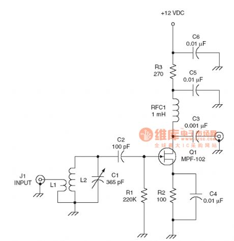
View full Circuit Diagram | Comments | Reading(1722)
the amplier circuit of the radio frequency :Common base JFET RF amplifier circuit
Published:2011/8/12 20:59:00 Author:Ariel Wang | Keyword: amplier, Common base , JFET, RF, amplifier
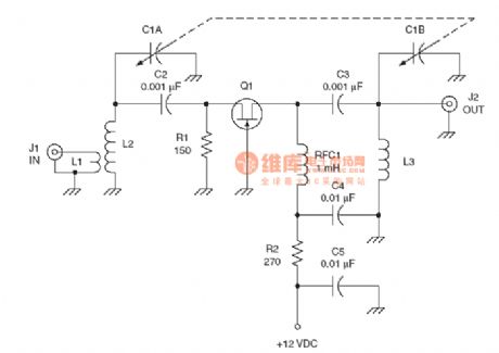
View full Circuit Diagram | Comments | Reading(1107)
the amplier circuit of the radio frequency :cascode RF amplifier circuit
Published:2011/8/12 20:58:00 Author:Ariel Wang | Keyword: amplier, RF, amplifier
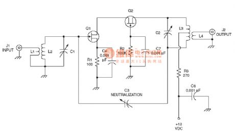
View full Circuit Diagram | Comments | Reading(1037)
Diagram of Precise Timer composed by LM567 and MP1826
Published:2011/8/9 18:00:00 Author:Vicky | Keyword: Precise Timer

LM567 is a frequency demodulating circuit. The circuit uses it as a two-frequency oscillator to generate the low-frequency pulse required by MP1826. The frequency of the central oscillating
ƒ0 is determined by C1, R2 and R3. ƒ0 is output by 3 pin of LM567, and 2 ƒ0 output by 8 pin can change the time constant of the circuit. ƒ0 varies between 0.01Hz to 500kHz. In this circuit, ƒ0 is 4Hz. When the circuit is on, MP1826 firstly reset, and meanwhile D1 go out after twinkling several times. In the low-frequency pulse input MP1826, pin 10 changes to high level after T time, and pin 11 changes to high level while pin 10 changes to low level after another T2 time; pins from 12 to 17 work in the same manner. When the pin 8 is grounding, pin 24 changes to high level after a period of time of 105×T2. Then the timing of the circuit ends. If the parameters of the components remain unchanged, there are 18 grades of timing of the circuit. (View)
View full Circuit Diagram | Comments | Reading(1921)
Input choice relation table circuit
Published:2011/8/10 7:24:00 Author:Fiona | Keyword: Input choice relation
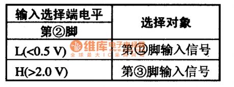
electrical level of the input choice terminal
selection objects
the 2 pin
L (<0.5 V)
the 12 pin's input singal
H (>2.0 V)
the3pin's input singal (View)
View full Circuit Diagram | Comments | Reading(543)
FM Wireless Microphone Circuit Diagram
Published:2011/8/9 18:01:00 Author:Vicky | Keyword: FM , Wireless Microphone

The following measures are taken to promise a clear voice of the microphone: the output signal of MIC is first sent to BG1 to be amplified. R1 and C1 is the additional pre-emphasized high-pitch sound circuit. C2 and C3 is the input and output coupling capacitance of tube BG1, the value of which is relatively lower to reduce the low-pitch sound and raise the mid and high sound. The diodes D3 and D4, which is connected in parallel in the BG1 output end , and the circuits C4 and C7, make use of the feature of the internal resistance ‘s being lower when the diodes are conducted in forward direction and influence the strong signal by limiting the amplitude. However, the regular signals remains unaffected. (View)
View full Circuit Diagram | Comments | Reading(3086)
Format control relation figure circuit
Published:2011/8/9 23:43:00 Author:Fiona | Keyword: Format control relation
SYS1’S 11 pin
SYS2’S 10 pin
COLOR SYSTEM
L
L
PALM
L
H
PALB、G、H、D、I
H
L
NTSCN
H
H
PALN (View)
View full Circuit Diagram | Comments | Reading(434)
Output choice relation table circuit
Published:2011/8/10 7:18:00 Author:Fiona | Keyword: Output choice relation
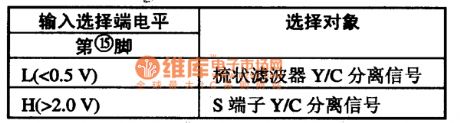
electrical level of the input choice terminal
selection objects
the 15 pin
L (<0.5 V)
comb type filter Y/C separation signal
H (>2.0 V)
S terminal Y/C separation signal (View)
View full Circuit Diagram | Comments | Reading(623)
Ultrasonic remote light switch circuit diagram
Published:2011/8/9 18:03:00 Author:Vicky | Keyword: ultrasonic, remote light switch
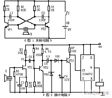
Picture 1 is a emitter circuit. The circuit uses discrete devices. VT1, VT1, R1, R2, R3, R4 , C1 and C2 constitute a self-excitation multivibrator. Ultrasonic emitting device B is connected in the collector loop of VT1 and VT2 to conduct push-pull work. The time of loop is often determined by R1, C1, R4 and C2. The resonance frequency of ultrasonic receptor device B triggers the multivibrator circuit. Hence, the circuit can work under optimized frequency.
Picture 2 is a receiving circuit, JFET VT1 constitutes high-input resistance amplifier, which performs better working with ultrasonic receptor device B and obtains higher receiving sensitiveness and better frequency-selecting performance. (View)
View full Circuit Diagram | Comments | Reading(1512)
Positive buck /boost type LED constant current driver circuit
Published:2011/7/20 6:51:00 Author:Fiona | Keyword: buck /boost, constant current, driver
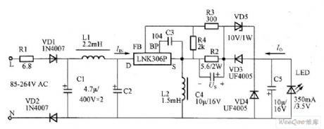
working principleThe input circuit consists of the fusible resistor R1,VD1,VD2,C1,CZ and filter inductor u;power adjustment circuit consists of LNK3OGP,energy storage inductor L2,VD3,R2,C4 and C5.When LNK306 turns on, the input current I constitutes a loop through (LNK306) D → (LNK306) S → L2 → C2 (-) and stores the input current IIN in inductor L2 (the inductor current linear increases by UI / LI),the polarity is that up is positive and under is negative;when LNK306 is off,it can't be mutated because of the inductor current(inductor current decreases linearly by UI/L1),the polarity is that up is negative and under is positive;the energy stored in L2 constitutes a loop through by the lower end of L2(ground) →LED (load) →VD3 →R2 →the upper end of L2.
(View)
View full Circuit Diagram | Comments | Reading(4329)
Light control automatic energy-saving LED lights circuit
Published:2011/7/20 7:33:00 Author:Fiona | Keyword: Light control, automatic energy-saving


Circuit is shown in Figure 1,electrical schematic diagram is shown in Figure 2. The voltage AC220V is reduced by C3,R3 discharges,VD1 and VD2 rectify,C2 and C1 filter and get a smooth direct current,the voltage-regulator diode stabilizes the voltage in 6V and supplys the power for MC1455P1G and photosensitive resistor.In the daytime,photosensitive resistor RG is small in the light,② and ⑥ pins of MC1455P1G input high level,③ pin outputs low level,the relay J2 is off,the contact of J1-1 does not turn on, 220V voltage is not added on the capacitor C5,so the LED is not bright.
(View)
View full Circuit Diagram | Comments | Reading(2044)
DC tachometer generator and single chip microcomputer interface circuit
Published:2011/7/20 7:07:00 Author:Fiona | Keyword: DC tachometer generator, single chip microcomputer, interface
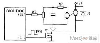
Figure is DC tachometer generator and single chip microcomputer interface circuit.In this system,it produces the PWM signal through the single chip microcomputer mouth to control the rotate speed of DC tachometer generator.Adding DC tachometer generator at the shaft of DC generator is used for measuring the motor's rotate speed,the tachometer generator output is analogue value,so it must A / D convert the output signal into digital tachometer signal,the tachometer signal compares with the given PWM signal through single chip microcomputer,it is used for acceleration or deceleration,thus forms the motor's closed-loop control system.
(View)
View full Circuit Diagram | Comments | Reading(696)
Diagram of Electronic Ballast Circuit composed of UBA2014
Published:2011/8/9 18:05:00 Author:Vicky | Keyword: Electronic Ballast

36W electronic ballast circuit diagram is shown in the above picture. When the power supply AC is on, it can charge capacitance C2 in the pin VDD of UBA2014 via the current of resistances R12 and R11. When the voltage of C2 rises to 13V, VCO inside the oscillator begins vibrating, and half-bridge power level composed by Q1 and Q2 generates output. When the oscillator begins working, the frequency is fmax=100kHz, and then it soon goes down to preheat frequency fpn. The preheat time is determined by R1 and R5. When R1 equals 33kΩ, and C5 equals 330nF, the preheat time tph equals 1.8 seconds. Once the preheat is over, the output frequency of ballast goes down again. During this procession, series circuit LC composed by output ends L1 and C15 begins vibrating, and then a high-voltage pulse is generated in the ends of C15, which goes through the light tube and then ignites. The frequency of oscillator reduces to fmin=40kHz. (View)
View full Circuit Diagram | Comments | Reading(2927)
Remote Control TX7004
Published:2011/8/9 17:30:00 Author:Vicky | Keyword: Remote Control

Product Specification:
Modulation mode: ASK/OOK (amplitude modulation)
Work voltage: DC 12V (27A/12V Battery)
Work current: 10mA
Work frequency: 315;433MHZ;(stable frequency for audiometer)
Transmission range: >200M (in spacious area, the sensibility of the receptor is above -100dbm)
Coding type: fixed/scroll/learning code
Key button: alternative between key 2 and key 4
Color of appearance: black
Coding types: coder and decoder: PT2260/PT2262 (pad); learning code: eV1527/PT2240B/scroll code: HCS101/HCS301
Product features:
Cheap; small size of the handle of emitter; exquisite appearance; power-saving; stable work performance; black appearance; settable rubber mat number. (View)
View full Circuit Diagram | Comments | Reading(699)
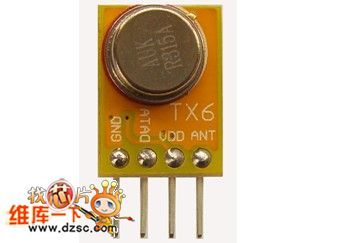
ASK/OOK Emitter module TX6
Published:2011/8/9 17:31:00 Author:Vicky | Keyword: ASK/OOK Emitter module

The module is composed by 315MHz or 433.92MHz audiometer oscillator. It belongs to ASK modulation emitter. It can be matched with frequently-used super-regenerative receiving circuit and superheterodyne receiving circuit. The frequency-stability is relatively high. It can be connected with coding chips and data transmission end in the outer side. It only consumes current when the button is pressed down, otherwise it consumes no current. It is easy to use.
Product specification
Communication mode: ASK amplitude modulation
Working frequency: 315MHZ~433.92MHZ
Static current: ≤0.1UA
Emitting current: 10mA
Working voltage: DC 3~12V
Working temperature: -20℃~+60℃
Size of appearance: 11x16x5.5MM
Frequency Stability: ±75KHZ
Emitting Power: 15dbm
Emitting distance: 500m (in the open space)
Emitting rate: 3KB/SInput signal: TTL electrical level (View)
View full Circuit Diagram | Comments | Reading(847)
Superheterodyne receiving module RXB4
Published:2011/8/9 17:33:00 Author:Vicky | Keyword: Superheterodyne Receiving Module
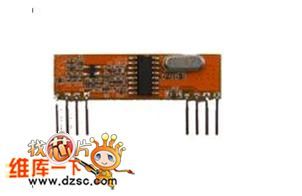
The module uses crystal frequency stabilization technology. It has relatively high frequency stability and uses SYN400R as the superheterodyne receptor. The receiving sensitiveness is high, the performance is stable, the current is low, the usage is easy, the size is small and it is cheap. The short antenna can be connected in the outside so that it is convenient to use. It can transmit direct current to the 2500BPS signal.
Product specification
Working voltage: DC 2.7~5.5V
Transmission rate: 2~4KBPS
Working mode: ASK amplitude modulation
Working current: 5MA
Receiving sensitiveness: -105dBm
Size of appearance: 43×12×5mm
Working temperature: -40℃~+85℃
Working frequency: 315 MHz;433 MHz;
Output frequency stability: ±30PBM
Output signal: CMOS electrical level
Ranking of pins: GND、DATA、DATA、+5V 、 +5V、GND、GND、ANT
Function of pins: GND: ground connection DATA: receiving data outputDATA: receiving data output+5V : working power,DC 5V ; +5V : working power,DC 5V ; GND: ground connectionGND: ground connection ANT: antenna
(View)
View full Circuit Diagram | Comments | Reading(645)
Superheterodyne receiving module RXB3
Published:2011/8/9 17:35:00 Author:Vicky | Keyword: Superheterodyne receiving module
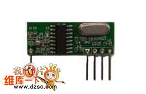
The module uses crystal frequency stabilization technology. It has relatively high frequency stability and uses SYN400R as the superheterodyne receptor. The receiving sensitiveness is high, the performance is stable, the current is low, the usage is easy, the size is small and it is cheap. The short antenna can be connected in the outside so that it is convenient to use. It can transmit direct current to the 2500BPS signal.
Product specification
Working voltage: DC 2.7~5.5V
Transmission rate: 2~4KBPS
Working mode: ASK amplitude modulation
Working current: 2MA
Receiving sensitiveness: -99dBm
Size of appearance: 30×11×5mm
Working temperature: -40℃~+85℃
Working frequency: 315 MHz;433 MHz;
Output frequency stability: ±30PBM
Output signal: CMOS electrical level
Ranking of pins: ANT、 +5V、SHUT、DATA、GND
Function of pins: ANT: antenna
+5V : working power DC 5V ; SHUT: power-saving module; DATA: receiving data output VSS: ground connection
(View)
View full Circuit Diagram | Comments | Reading(652)
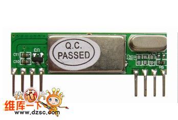
Superheterodyne receiving module RXB5
Published:2011/8/9 17:36:00 Author:Vicky | Keyword: Superheterodyne receiving module
The module uses crystal frequency stabilization technology. It has relatively high frequency stability and uses RXB5 as the superheterodyne receptor. The receiving sensitiveness is high, the performance is stable, the current is low, the usage is easy, the size is small and it is cheap. The short antenna can be connected in the outside so that it is convenient to use. It can transmit direct current to the 9600BPS signal.
Product specification
Working voltage: DC 2.7~5.5V
Transmission rate: 0KBPS~9.6KBPS
Working mode: ASK amplitude modulation
Working current: 6mA
Receiving sensitiveness: -102dBm
Size of appearance: 30×11×5mm
Working temperature: -20℃~+70℃
Working frequency: 315 MHz; 433 MHz;
Output signal: CMOS electrical level
Ranking of pins: ANT、 GND、GND、DATA、VDD
Function of pins: ANT: antenna
GND: ground connectionGND: ground connectionDATA: receiving data output, and presenting high-resistance state when there is no signalVDD : working power
(View)
View full Circuit Diagram | Comments | Reading(698)
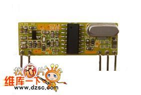
Superheterodyne receiving module RXB6
Published:2011/8/9 17:39:00 Author:Vicky | Keyword: Superheterodyne receiving module
This RF wireless high-frequency receiving module, RXB6, is of high sensitiveness, which reaches -110dBm. It adopts ASK receiving mode, which is available for remote control, far- end control, remote control vehicle, data transmission, anti-theft alarm, home appliance control, wireless toy, vehicle-burglar alarm, wireless backup radar, remote garage gate control , remote motor-driven curtain, flexible door , remote strobe control. It is also an ideal choice GSM/GPS vehicular system set, industry control and systems of high complicated environmental requirement. It can take the place of infrared receptor. It can receive signals from omnidirectional direction and is easy to be added to general remote controls.
Key Feature:
315/433.92/868/914.5MH receiving module
Built-in AGC
Low working voltage: 3.0V~5.5V
Low current: 315MHZ/433.92MHZ(it is available to be connected to power-saving mode in the outside and the start-up time is 250µs; the low-current shutdown mode is 30mA, which effectively saves power)
High sensitiveness: -110dBm
Working temperature: -40℃~+85℃
Size of the appearance: 43.2×12.3×5mm (View)
View full Circuit Diagram | Comments | Reading(1563)
| Pages:570/2234 At 20561562563564565566567568569570571572573574575576577578579580Under 20 |
Circuit Categories
power supply circuit
Amplifier Circuit
Basic Circuit
LED and Light Circuit
Sensor Circuit
Signal Processing
Electrical Equipment Circuit
Control Circuit
Remote Control Circuit
A/D-D/A Converter Circuit
Audio Circuit
Measuring and Test Circuit
Communication Circuit
Computer-Related Circuit
555 Circuit
Automotive Circuit
Repairing Circuit