
Circuit Diagram
Index 573
timer circuit fixing preset time
Published:2011/7/27 8:25:00 Author:Fiona | Keyword: Fixing preset time, timer
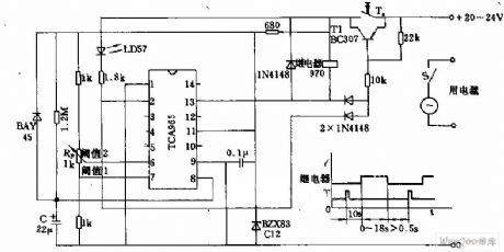
The 13 pin between Threshold value 1 and 2 absorbs the transistor's base current. If relay releases,it starts the switch process again through pressing the button after restoring time 0.5 S.Window discriminator TCA965 can constitute a timer.Capacity C which decides the time charges after pressing the button Ta ,transistor T1 gets the base current from TCA965's 2 pin,power supplys current.Rectification process times 10 S in advance.In some period indicator light LD57 is bright. When capacitor's charging voltage exceeds threshold value 1 ,the relay is closed.But when capacitor's charging voltage exceeds threshold value 2 after rectifying by potentiometer RP,the relay releases again. Relay's pick-up duration can be adjusted in 0 ~ 18 S.
(View)
View full Circuit Diagram | Comments | Reading(1900)
Telephone electronic coded lock circuit
Published:2011/7/27 8:27:00 Author:Fiona | Keyword: electronic coded lock
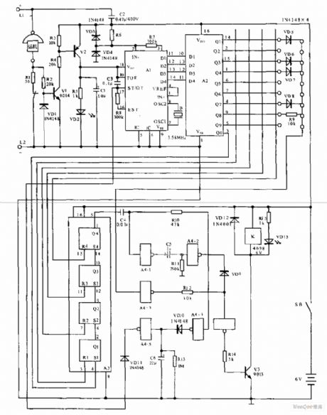
Telephone electronic coded lock circuit is shown as above,the electronic coded lock is suitable for double audio circuits.After the phone adds this coded lock, when you call out,you must use the buttons on the phone to press the four pre-programmed password,then you can make a call.If the password is error, the phone can not dial out. When the exterior line is incoming call,the phone can receive the ring signal normally,picking machine can response.When the electronic coded lock circuitis connected toexterior line to be used,we mustmeasure the positive and negative polarities of outside feeder,then connect the positive pole to L1 and connect L2 to the negative pole,the phone is connected to the the phone location in electronic coded lock circuit.
(View)
View full Circuit Diagram | Comments | Reading(1606)
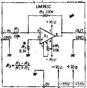
The circuit of DC inverting amplifier whose gain is decided by the ratio
Published:2011/7/27 8:24:00 Author:Fiona | Keyword: DC reversed-phase amplifier
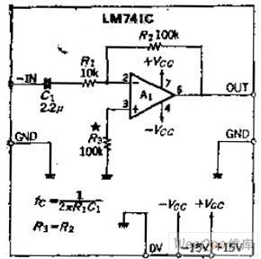
Circuit WorkBecause the OP amplifier inverting input is grounded, inverting input in the linear operating range is zero level. So the input resistance of the circuit is R1, if R2 remains unchanged, the input resistance decreased with the increased gain. Due to there has input bias current IB flowing through in the OP amplifier, if removing the resistance R3, it will produce additional bias. If you are using FET input type OP amplifier, you can save R3.
Because the magnification is 10 times,the circuitneeds toincrease the offset adjustment circuit, in the 741-type OP amplifier, the circuit connects the 10 k ohms variable resistor between 1,5 lead.
(View)
View full Circuit Diagram | Comments | Reading(614)
The AC inverting amplifier circuit that maintain bias by the selected gain
Published:2011/7/27 8:22:00 Author:Fiona | Keyword: selected gain, AC inverting amplifier, maintain bias
Circuit function
Dispense with amplified DC signal, it is in series with a blocking capacitor C1 at the input resistance,it can make the offset drift neglected. Even though the AC gain of amplifier is high, the output is still DC working, OP amplifier is only used as a simple amplification devices. Using R3 = R2 to achieve input current bias, but because of the DC gain L, therefore, this requirement is not too strict, such as the resistance of R2 is small, R2 can be removed. Increasing the capacitor C1, it can get low-frequency time constant, the frequency F0 is 1 / N, C1.R1, phase shift is 45 degrees, characteristic curve downs 1 / √ 2 (3DB). Therefore, to obtain flat characteristics, it should be in accordance with FO(1 / 3 ~ 1 / 5) to determine the C1 value.
(View)
View full Circuit Diagram | Comments | Reading(602)
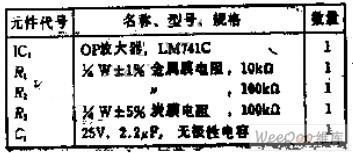
Simplified bridge type thermosensitive temperature measurement circuit
Published:2011/7/27 8:21:00 Author:Fiona | Keyword: Simplified bridge type, thermosensitive temperature measurement

Circuit Work
Four-leg resistors are equal, this is the most common method that the bridge circuit selects parameters,each leg of the circuit resistance takes 10K. VR1 is a variable resistor, and itsfunction is to make the output voltagebe 0 at the required temperature, when the thermistor resistance and the arm resistance are equal, adjust VR1 so that the bridge is balance.
Thermistor resistance falls due to temperature rises, the differential amplifier output will rise, the output voltage depends on the thermistor constant B or increasing the voltage at the bridge. (View)
View full Circuit Diagram | Comments | Reading(961)
choosing operation mode by the input terminal adding and subtraction circuit
Published:2011/7/27 8:21:00 Author:Fiona | Keyword: input terminal, adding, subtraction, operation mode


Circuit function
This is the PSD of match using silicon photodiodes.In order to reduce the error because of receiving flux,it usually carries out the operation A + B, and thus to control the laser diode power. This circuit uses the common circuit module that can add and subtract, which has 3 inputs, but has different functions,for example, only the A and B input, it's a common additive A + B circuit; if it uses C to input and uses one between A and B,you can subtract.
Circuit Work
This addition and subtraction circuit is composed of the inverse OP amplifier circuit, the output voltage EO can express by the following formula:
Under this formula, if assuming the resistance R1 ~ R6 are equal, you can to do the addition and subtraction operations that the magnification is 1.
In the inverting amplifier, the input resistor is the input impedance, if it needs high input resistance, OP amplifier should be replaced by BI-FET type, such as the TL082, etc., and removes the resistors R7, R8. (View)
View full Circuit Diagram | Comments | Reading(653)
2 W x 2 power amplifier(LM1877)circuit
Published:2011/8/8 9:07:00 Author:Fiona | Keyword: 2 W x 2 power amplifier

Shown in the figure,the circuituses on,under symmetrical structure and has two way signal which is added respectively to the two op-amp non-inverting input ends of LM1877,its output end’s external way is same with the input end: it uses 2.7 Ω resistor and 0.1 u F to form the high frequency filter circuit to prevent the high frequency of self-excited; coupling capacitor Co (470 u F) and load resistor ZL (loudspeaker:8Ω) concert the output power into voice to output, and the magnitude of Co and ZL circuit is also determined to the circuit’s lower-cut-off frequency fL,the relationship between this three is: fL=1/(2πZLCo),corresponding to the parameters in the figure,its fL = 42 Hz.
(View)
View full Circuit Diagram | Comments | Reading(1361)
SN75322 dual positive and gate TTL-MOS driver circuit
Published:2011/8/8 9:05:00 Author:Fiona | Keyword: dual positive and gate, driver circuit
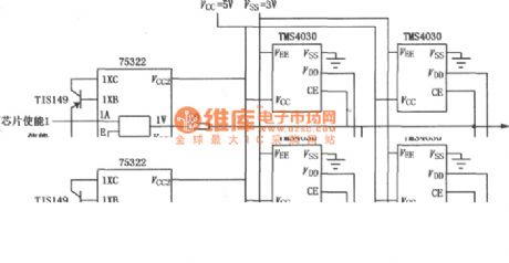
SN75322 is single dual positive and gate TTL-MOS driver circuit,which is used as an interface between TTL and high-voltage and high-current system.It uses TTL and MOS supply voltage,and can switch at a high speed.Its input is compatible with TTL and MOS circuits .It has a common strobe input. 5V power supply outputs are high impedance when vacancies. Output directly drives 4030 4K RAM,and needs two external PNP transistor while it is being used.The circuitthat SN75322 is used as a 4030MOS memory driver is shown as above.
(View)
View full Circuit Diagram | Comments | Reading(811)
The pin function circuit of TDA9210 integrated circuit
Published:2011/8/8 9:03:00 Author:Fiona | Keyword: pin function, integrated circuit
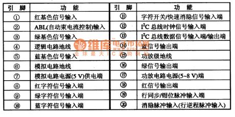
1. pin function
TDA9210 integrated circuit uses 20-pin biserial inline package , and its pin functions are listed in Table 70.
(View)
View full Circuit Diagram | Comments | Reading(524)
TDA9321 Integrated circuit pin functions and data circuit
Published:2011/8/8 9:01:00 Author:Fiona | Keyword: pin functions and data
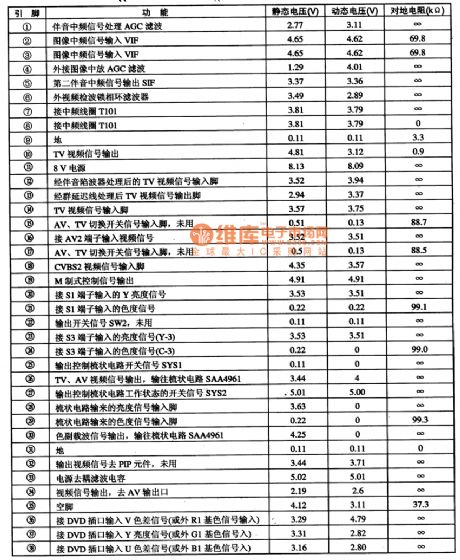
TDA9321 ——Intermediate frequency signal processing, field trip small signal processing, light-coloredhandle monolithic IC.TDA9321 is a small TV signal processing integrated circuit chip produced by PHLIPS, which is widely used in large-screen TV in the new multiplier, such as Changhong TD2000.1.FeaturesTDA9321 Integrated circuit contains image and sound IF circuit, small field scanning line signal processing circuit, luminanceand chrominance signal processing circuit, and other auxiliary functions circuit. The entire circuit completes the processing under I (2) C bus’s control.2.The whole pin functions and data TDA9321 IC uses 64-pin dual in-line package,which is applyed to Changhong color TV on the DT2000 frequency.And the integrated circuit ‘s pin functions are listed inTable 73.
(View)
View full Circuit Diagram | Comments | Reading(534)
The automatic charging, power supply dual-use device circuit (1)
Published:2011/8/1 22:04:00 Author:TaoXi | Keyword: Automatic, charging, power supply, dual-use, device

The automatic charging, power supply dual-use device circuit is as shown in the figure 4-2. IC1 is the three-port voltage stabilizer LM317T, it forms the adjustable voltage stabilization power supply, the output voltage can be adjusted in the range of 1.25V-20V through RP1; IC2 is the CD4060, it is designed as one kind of 14-stage binary addition calculator/oscillator, the timer and pulse generator is composed of this calculator/oscillator and the external components. IC3 is the NE555, it forms the simple automatic charging circuit; IC4 is the sampling controller that is composed of the four-two input NAND gate CD4011 to control the conversion of the charging current.
After the battery is installed, it gives a positive pulse to the pin-12 of IC2 through C6, the IC2 starts to oscillate, the oscillation frequency is about 1.8Hz that is decided by the R6 and R7.
(View)
View full Circuit Diagram | Comments | Reading(572)
The practical simple battery automatic charger circuit
Published:2011/8/1 22:03:00 Author:TaoXi | Keyword: Practical, simple, battery, automatic charger

The circuit principle of the charger is as shown in figure 4-18. The 220V AC city electricity is transformed, rectified and filted by this circuit to output the 20V direct current, and this current charges the battery through the three-port voltage stabilizer. The switching circuit TWH8778 can be used to detect the two-end voltage of the battery.
When the charging starts, the voltage of battery is not enough to conduct the TWH8778, the equivalent circuit is as shown in figure 4-19(a). The constant current charges the battery, the constant current value I0=12.5/R, R is one resistance value of the R1-R4. When the battery voltage increases to the set value, the circuit of figure 4-19(b) is automatically converted into the circuit of 4-19(c).
(View)
View full Circuit Diagram | Comments | Reading(693)
The safe and reliable multi-function charger circuit
Published:2011/8/1 22:04:00 Author:TaoXi | Keyword: Safe, reliable, multi-function, charger


The principle diagram of this charger is as shown in figure 5-16. The 220V city electricity is reduced by the transformer T, and it is bridge rectified by the diodes VD1-VD4 to output the 17V, 100Hz pulsating DC voltage, this DC voltage can supply the power to the charging circuit. The DC current is stabilized by IC1 to supply power to the time-base integrated circuit IC2(NE555), so the IC2(NE555) produces the oscillation, we can use the pulse signal which is output by the pin-3 to control the conduction and cut-off of the darlington tube which is composed of the VT1 and VT2. This circuit has the RP, the electric potential of the adjustable port of it can be used to set the recharging the battery benchmark voltage.
(View)
View full Circuit Diagram | Comments | Reading(932)
Clairvoyance charger (6V storage battery multi-function charger circuit)
Published:2011/7/26 20:10:00 Author:TaoXi | Keyword: Clairvoyance, charger, 6V, storage battery, multi-function, charger

The Clairvoyance charger circuit is as shown in figure 2-8, the unidirectional thyristor VS1 is used as the charge current tube of the storage battery GB, the VS2 can cut off the charging current when the storage battery is charging. When the power supply is charging, the relay K operates, the contact point 3 is connected with the contact point 2, the trigger port of VS1 gets the trigger voltage from the R1 and VD1 to conduct, the rectifier current charges the storage battery GB through the VS1. When the storage battery GB is charged to the set voltage, the VS2 conducts, so the VS1 trigger port point A's electric potential is lower than the cathode potential of VS2. VS1 cuts off, the storage battery GB stops charging. The LED can be used to show the charging.
(View)
View full Circuit Diagram | Comments | Reading(1020)
The sub-ultrasonic remote control switch circuit
Published:2011/8/1 22:03:00 Author:TaoXi | Keyword: Sub-ultrasonic, remote control switch

The sub-ultrasonic remote control switch circuit is as shown:
(View)
View full Circuit Diagram | Comments | Reading(566)
ZhongHua saloon car engine circuit 1
Published:2011/8/8 2:14:00 Author:TaoXi | Keyword: ZhongHua, saloon car, engine circuit

F54-ABS fuse (60A) F55-storage battery fuse (70A) F56-ignition fuse (60A) F60-start fuse (60A) R35-start relay H03-power connector U01UA-connection point, in the ABS wiring harness U02A1A-connection point, in the engine room left wiring harness U05PA/U14PA/U16PA/U17PA-connection points, in the dashboard wiring harness T1-connector of engine left wiring harness and dashboard wiring harness T13-ABS wiring harness and engine room left wiring harness connector T15-dashboard wiring harness and engine room left wiring harness connector T47-interface of engine room left wiring harness and power connector (View)
View full Circuit Diagram | Comments | Reading(624)
ZhongHua saloon car engine circuit 3
Published:2011/8/8 2:00:00 Author:TaoXi | Keyword: ZhongHua, saloon car, engine
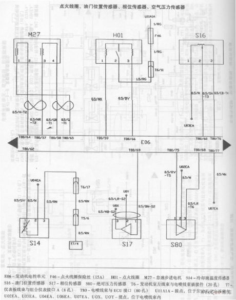
ZhongHua saloon car engine circuit
E06-Engine electronic control unit F46-ignition coil fuse(15A) H01-ignition coil M27-idle speed stepper motor S14-cooling fluid temperature sensor S16-throttle position sensor S17-phase sensor S80-absolute pressure sensor T6-engine room left wiring harness and EFI wiring harness connector T7-dashboard wiring harness and combination meter interface T80-EFI wiring harness and ECU interface U11A1A-connection point, in the left wiring harness of the engine U02EA,U03EA,U04EA,U06EA,U07EA,UOX,UOY-connection points, in the EFI wire harness (View)
View full Circuit Diagram | Comments | Reading(541)
ZhongHua saloon car ABS circuit 1
Published:2011/8/8 1:45:00 Author:TaoXi | Keyword: ZhongHua, saloon car, ABS
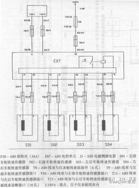
F20-ABS fuse(10A) E07-ABS electronic control unit J1-ABS electromagnetic valve relay S01-left front wheel revolution speed transducer S02-right front wheel revolution speed transducer S03-left rear wheel revolution speed transducer S04-right rear wheel revolution speed transducer T8-ABS wiring harness and dashboard wiring harness connector T9-ABS wiring harness and left front wheel revolution speed transducer interface T10-ABS wiring harness and right front wheel revolution speed transducer interface T11-ABS wiring harness and left rear wheel revolution speed transducer interface T12-ABS wiring harness and right rear wheel revolution speed transducer interface T18-dashboard wiring harness diagnosis interface U18PA-connection point of the dashboard wiring harness. (View)
View full Circuit Diagram | Comments | Reading(557)
The infrared remote control detector
Published:2011/8/1 22:06:00 Author:TaoXi | Keyword: Infrared, remote control, detector
Infrared remote control detector
(View)
View full Circuit Diagram | Comments | Reading(706)
The infrared remote control music socket circuit (1)
Published:2011/8/1 22:07:00 Author:TaoXi | Keyword: Infrared remote control, music socket
The infrared remote control music socket circuit is as shown, it is composed of the pulse oscillator circuit , the buffer stage and the driver stage.
Infrared receiving controller circuit:
(View)
View full Circuit Diagram | Comments | Reading(876)
| Pages:573/2234 At 20561562563564565566567568569570571572573574575576577578579580Under 20 |
Circuit Categories
power supply circuit
Amplifier Circuit
Basic Circuit
LED and Light Circuit
Sensor Circuit
Signal Processing
Electrical Equipment Circuit
Control Circuit
Remote Control Circuit
A/D-D/A Converter Circuit
Audio Circuit
Measuring and Test Circuit
Communication Circuit
Computer-Related Circuit
555 Circuit
Automotive Circuit
Repairing Circuit