
Circuit Diagram
Index 585
Voice Cycle Lights (the 2nd)
Published:2011/8/6 21:09:00 Author:Felicity | Keyword: Voice Cycle, Lights

Work of the circuit
The circuit consists of power circuits, voice circuits, astable oscillator, VCO / count divider and control implementation circuit. (It is showed in picture 1-109.)
Power circuit consists of Buck capacitor C6, resistor Rll, voltage regulator diode VS, VD rectifier diode and filter capacitor C5.
Voice circuit consists of Piezoelectric ceramics BC, transistors Vl, V2, potentiometer RPl, resistors Rl-R3 and capacitor Cl, C3.
Astable oscillator consists of Time-base integrated circuit lCl and resistors R5, R6, and capacitor C2 potentiometer RP2.
VCO / count divider consists of Specific integrated circuit IC2 and lighting control resistor R7, capacitor C4.
Control implementation circuit consists of Resistor R8-RlO, VLl-VL3-emitting diode and thyristor VTl-VT3. (View)
View full Circuit Diagram | Comments | Reading(601)
Automatic Sprinkler Controller (the 2nd)
Published:2011/8/6 21:14:00 Author:Felicity | Keyword: Automatic Sprinkler, Controller

Work of the circuit
The circuit consists of power circuit, switching control circuit, astable oscillator circuit and control implementation circuit. (It is showed in picture 4-81.)
Power circuit consists of power switch Sl, the power transformer T, to bridge rectifier UR and filter capacitor Cl.
Switching control circuit consists of humidity sensors, sampling tubes Vl, composite amplifier tube V2, V3, power filtering tube and resistors Rl-R4.
Astable oscillator circuit consists of Time-base integrated circuit lC and external RC components.
Control implementation circuit consists of transistor V4, LED VL, VT, and manual control thyristor switch S2. (View)
View full Circuit Diagram | Comments | Reading(657)
Voice Cycle Lights (the 1st)
Published:2011/8/6 21:08:00 Author:Felicity | Keyword: Voice Cycle, Lights

Work of the circuit
The circuit consists of power circuits, voice circuits, oscillator, pulse counting distributor and control implementation circuit. (It is showed in picture 1-108.)
Power circuits consists of buck capacitor Cl, resistors Rl, voltage regulator diode VS, filter capacitor C2 and diode rectifier VD.
Voice circuits consists of piezoelectric transducer BC, the transistor V, resistors R2, R3, capacitor C3 and potentiometer RPl.
Oscillator consists of time-base integrated circuit ICl, resistor R4, capacitor C4 and potentiometer RP2.
Pulse counting distributor consists of count / pulse distributor circuit IC2.
Control implementation circuit consists of thyristor VTl-VTlO, resistors R5-R14 and lanterns HLl-HLlO.
(View)
View full Circuit Diagram | Comments | Reading(647)
Automatic Sprinkler Controller (the 1st)
Published:2011/8/6 21:12:00 Author:Felicity | Keyword: Automatic Sprinkler Controller (the 1st)

Work of the circuit
The circuit consists of clock timing controller, a single-shot, flip flop, electronic switch, self-excited multivibrator, counter, solenoid valve control circuit and power circuit. (It is showed in picture 4-80.)
Clock timing controller consists of digital electronic clock integrated circuit ICl, IC2, LCD liquid crystal displays, quartz crystal BCl, BC2, adjustable button Sl-S4, battery GBl, GB2 and capacitors Cl-C6.
Single-shot consists of dual D flip-flop within the D flip-flop integrated circuit IC3 Al and peripheral components.
Flip flop consists of D trigger A2 within IC3.
Electronic switch consists of High-power switch integrated circuit IC4.
Self-excited multivibrator consists of time-base integrated circuits IC5 and peripheral components.
Counter consists of counter / divider integrated circuit IC6 and peripheral components.
Solenoid valve control circuit consists of electronic switch integrated circuit IC7. ICI5, relay Kl-K9, LED VLl-VL9, solenoid valve YVl-YV9 and resistors R8-R25.
Power circuit consists of electronic switch integrated circuit IC7. ICI5, relay Kl-K9, LED VLl-VL9, solenoid valve YVl-YV9 and resistors R8-R25.
(View)
View full Circuit Diagram | Comments | Reading(1127)
The circuit diagram of active low-pass filter(LM102)
Published:2011/8/6 0:02:00 Author:Felicity | Keyword: active low-pass filter

The figure shows the circuit diagram of active low-pass filter (LM102).The cutoff frequency fc=10 kHz. In the circuit, the ratio of R1 to R2 or of C1 to C2 can be any value. In this circuit, R1=R2 and C1=C2. C1=C2 and R1=R2 can also be okay. (View)
View full Circuit Diagram | Comments | Reading(1826)
74 Series digital circuit of 74LS395A,74F395 4-bit cascadable shift register (tristate)
Published:2011/8/1 22:50:00 Author:Lucas | Keyword: 74 Series , digital circuit , 4-bit cascadable, shift register , tristate

It is the tri-state 4-bit cascaded parallel input and output shift register; 74LS395A absorption current is three times greater than 74LS395. When output control is high, the tri-state output disable is high impedance, but the timing work and QD output of the register is not affected.
a~ d = the corresponding steady input level of A~ D. QA0~ QD0= the corresponding level of QA~QD before the establishment of steady-state input conditions. QAn~ QDn= the corresponding level of QA~ QD at the latest time hopping.
(View)
View full Circuit Diagram | Comments | Reading(1099)
74 Series digital circuit of 74LS384, 74F384 8-bit × 1-bit complement multiplier
Published:2011/8/2 1:00:00 Author:Lucas | Keyword: 74 Series , digital circuit , 8-bit × 1-bit , complement multiplier


2's complement multiplication; it is only multiplied by the absolute value; it can be cascaded to any bit; 8-bit multiplied data parallel input; multiplier data serial input; product data serial output; LS384 typical maximum clock frequency is 40MHz; when is is cascaded,the output of a circuit is connected to K input of the next circuit, and the circuit contains the highest level can be indicated by the model input.
(View)
View full Circuit Diagram | Comments | Reading(1562)
74 Series digital circuit of 74LS373, 74ALS373 octal D-latch(tristate)
Published:2011/8/1 23:01:00 Author:Lucas | Keyword: 74 Series , digital circuit , octal D-latch, tristate

Tristate output; the load full parallel access; buffer control input; 74LS363 is similar to 74LS373, but has the high VOH with MOS interface.
Q0 = the output level before establishing the steady-state input conditions.
(View)
View full Circuit Diagram | Comments | Reading(5036)
74 Series digital circuit of 74LS362 four-phase clock generator / driver
Published:2011/8/1 22:56:00 Author:Lucas | Keyword: 74 Series , digital circuit , four-phase clock generator , four-phase driver
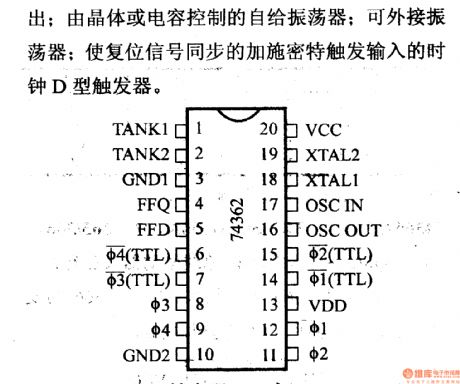
It is used as TMS9900 or other microprocessor clock generator/ driver; high four-phase output; complementary TTL four-phase output; it is the self-support oscillator controlled by the capacitor and crystal; it can connect external oscillator; the reset signal is synchronized by the clock D flip-flop with the Schmitt trigger input.
(View)
View full Circuit Diagram | Comments | Reading(1718)
74 Series digital circuit of 74LS354/356 8-to-1 data selector(tristate with address latching)
Published:2011/8/2 0:43:00 Author:Lucas | Keyword: 74 Series, digital circuit , 8-to-1 data selector, tristate , address latching
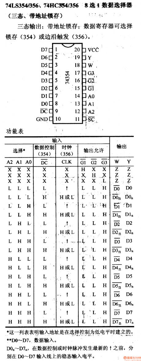
This list shows that the input address is established when the control is low. D1 ~ D7 are the data input. D0n ~ D7n are the steady state input level in D0 ~ D7 line before the latest increasing of the data control or clock pulse.
Three-state output with address latching; data register can choose data latch(354) or edge-triggered (356).
(View)
View full Circuit Diagram | Comments | Reading(735)
74 Series digital circuit of 74LS352, 74F352 dual 4-to-1 data selector(inverting)
Published:2011/8/1 20:49:00 Author:Lucas | Keyword: 74 Series , digital circuit , dual 4-to-1 , data selector, inverting

The selecting inputs A and B are used in common.
(View)
View full Circuit Diagram | Comments | Reading(797)
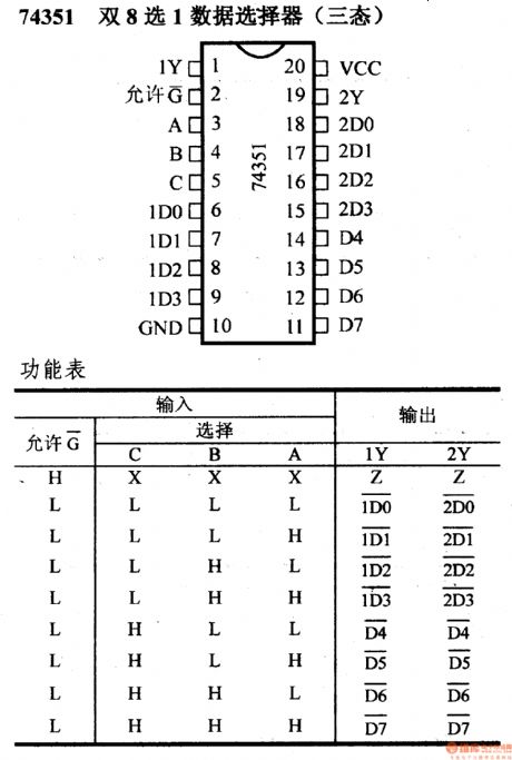
74 Series digital circuit of 74351 dual 8-to-1 data selector(tristate)
Published:2011/8/1 20:43:00 Author:Lucas | Keyword: 74 Series, digital circuit , dual 8-to-1 , data selector, tristate
View full Circuit Diagram | Comments | Reading(672)
74 Series digital circuit of 74LS325 dual VCO(two-phase output)
Published:2011/8/1 20:34:00 Author:Lucas | Keyword: 74 Series, digital circuit , dual VCO, two-phase output

There are two independent voltage-controlled oscillators; output frequency is determined by the external components; it can works at any frequency between 0.12Hz and 30MHZ; it has the complementary output.
(View)
View full Circuit Diagram | Comments | Reading(1072)
74 Series digital circuit of 74LS299, 74S299 8-bit bidirectional universal shift/storage registers
Published:2011/8/2 4:36:00 Author:Lucas | Keyword: 74 Series , digital circuit , 8-bit bidirectional, universal shift, storage registers
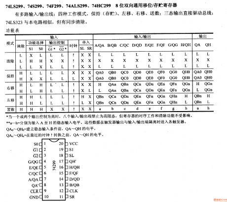
It has multi-road / output lines and four modes to maintain (store) left, right shift and output number; three-state outputs can directly drive the bus; 74LS323 is similar to the circuit, but it has the synchronous clear function. When one or two output controlling is high, eight input / output ends against in high-impedance state, but the timing register and cleaning functions are not affected. The data is input to each trigger when the flip-flop output and input ends are isolated.
QA10~QH0 is the level of QA~QH before the establishment of steady-state input conditions. QAn~QHn=the level of QA~QH before the latest time hopping.
(View)
View full Circuit Diagram | Comments | Reading(1567)
74 Series digital circuit of 74LS323,74S323 8-bit bidirectional universal shift/storage registers
Published:2011/8/2 4:34:00 Author:Lucas | Keyword: 74 Series, digital circuit , 8-bit bidirectional , universal shift, storage registers

It has multi-road / output lines and four modes to maintain (store) left, right shift and output number; three-state outputs can directly drive the bus; 74LS299 is similar to the circuit, but it has the asynchronous reset. When one or two output controlling is high, eight input / output ends against in high-impedance state, but the timing register and cleaning functions are not affected. The data is input to each trigger when the flip-flop output and input ends are isolated.
QA10~QH0 is the level of QA~QH before the establishment of steady-state input conditions. QAn~QHn=the level of QA~QHbefore the latest timehopping.
(View)
View full Circuit Diagram | Comments | Reading(854)
74 Series digital circuit of 74LS322,74F322 sign-extended 8-bit shift register
Published:2011/8/2 3:55:00 Author:Lucas | Keyword: 74 Series, digital circuit , sign-extended 8-bit , shift register
Multiple input / output; tri-state outputs can directly drive the bus; it has signed extended function; it can be direct unconditional cleared. When the output allows for high, eight input / output ends can not be in a high-impedance state, but does not affect the timing operation or clear of registers, for example, if the register allows the input and S / P input, the clear input are low, the register is removed, and eight input / output ends can not be in a high-impedance state.
QA0 ...QH0= QA ...QH level before the establishment of steady-state input conditions.
D0, D1=the steady input level ofinput ends D0, D1
a..h =the steady input level of the input ends of A to H.
(View)
View full Circuit Diagram | Comments | Reading(746)
74 Series digital circuit of 74LS295B 4-bit bidirectional universal shift register (tristate)
Published:2011/8/2 4:24:00 Author:Lucas | Keyword: 74 Series , digital circuit , 4-bit bidirectional , universal shift register , tristate


Absorption current is three times greater than LS295A; parallel input, parallel output; it has three operation modes with parallel register, and the right shift(direction is from QA to QD), left shift(the direction is from QD to QA). Data is input at the D-side.
a, b, c, d = the corresponding steady input level of A, B, C, D.
QA0, QB0, QC0, QD0= the corresponding level of QA, QB, QC, QD before the establishment of steady-state input conditions.
QAn, QBn, QCn= the corresponding level of QA, QB, QC at the latest time hopping.
(View)
View full Circuit Diagram | Comments | Reading(1153)
74 Series digital circuit of 74LS294,74HC294 programmable divider / digital timer
Published:2011/8/1 20:44:00 Author:Lucas | Keyword: 74 Series , digital circuit , programmable divider , digital timer

View full Circuit Diagram | Comments | Reading(969)
74 Series digital circuit of 74LS292,74HC292 programmable divider / digital timer
Published:2011/8/1 20:45:00 Author:Lucas | Keyword: 74 Series , digital circuit , programmable divider , digital timer

View full Circuit Diagram | Comments | Reading(908)
74 Series digital circuit of 74285 4 × 4-bit parallel binary multiplier(low topological product)
Published:2011/8/1 20:24:00 Author:Lucas | Keyword: 74 Series , digital circuit , 4 × 4-bit parallel , binary multiplier, low topological product

OC output can generate low topological product; 74284 and 74285 can be used in a group. 4 × 4-this part of the product is combined with a full adder.
(View)
View full Circuit Diagram | Comments | Reading(2018)
| Pages:585/2234 At 20581582583584585586587588589590591592593594595596597598599600Under 20 |
Circuit Categories
power supply circuit
Amplifier Circuit
Basic Circuit
LED and Light Circuit
Sensor Circuit
Signal Processing
Electrical Equipment Circuit
Control Circuit
Remote Control Circuit
A/D-D/A Converter Circuit
Audio Circuit
Measuring and Test Circuit
Communication Circuit
Computer-Related Circuit
555 Circuit
Automotive Circuit
Repairing Circuit