
Circuit Diagram
Index 597
BASIC_CLASS_B_PUSH_PULL_OUTPUT
Published:2009/7/14 22:30:00 Author:Jessie
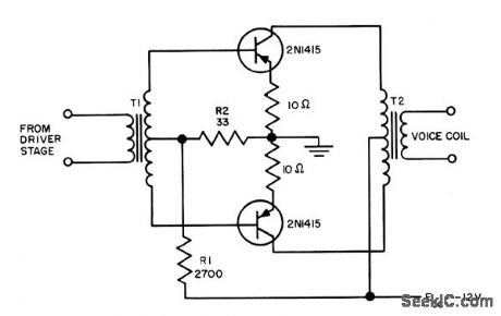
Design procedures are given. Resistor in emitter leads prevent thermal runaway when ambient temperature is below 55℃ .- TransistorManual , Seventh Edition, General Electric Co.,1964,p 242. (View)
View full Circuit Diagram | Comments | Reading(1108)
VOLTAGE_CONTROLLED_DELAY_GENERATOR
Published:2009/7/14 21:36:00 Author:May
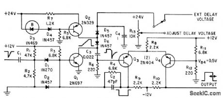
Accuracy is 0.7%,with high stability. Used in radar range tracker, which requires accurate voltage analog of time between out going pulse and incoming echo.-C. K. Friend and S. Udalov, Stabilized Delay Circuit Provides High Accuracy, Electronics, 34:15, p 78-80. (View)
View full Circuit Diagram | Comments | Reading(726)
CASCADED_UJT_RELAXATION_OSCILLATOR_DIVIDER
Published:2009/7/14 21:36:00 Author:May

Class C Hartley master oscillator serves for synchronizing three basic relaxation oscillators that would otherwise be free-running. Dividers remain locked over temperature range of 0 to 70℃.- Transistor Manual, Seventh Edition, General Electric Co., 1964, p 342. (View)
View full Circuit Diagram | Comments | Reading(1574)
LED_INDICATES_SIGNAL_LEVEL
Published:2009/7/14 22:32:00 Author:Jessie

Circuit is adjusted so opamp turns on LED at desired signal level as set by R1 Opamp is operated without feedback resistor to have maximum gain, so small input signal produces very large output signal Values shown for R2 and R3 give turn-on voltage of 0.9 V for LED.-F. M. Mims, Integrated Circuit Projects, vol. 4, Radio Shack, Fort Worth, TX, 1977, 2nd Ed., p 70-75. (View)
View full Circuit Diagram | Comments | Reading(939)
SILICON_CONTROLLED_SWITCHES_DIVIDE_FRE_QUENCY_BY_100
Published:2009/7/14 21:35:00 Author:May


Each 3N60 stage divides input frequency by 10 while serving as relaxation oscillator, for frequencies from 250 kc down to fraction of cycle. Circuit can also be used as sawtooth generator.-R. J. Wold, 4-lerminal Controlled Switch Divides Frequencies by 10, Electronics, 37:18, p 81-82. (View)
View full Circuit Diagram | Comments | Reading(688)
TWO_CHIP_TUNER
Published:2009/7/14 22:32:00 Author:Jessie
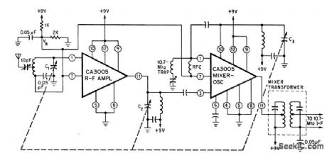
Use of additional RCA integrated-circuit chip as r-f amplifier improves gain and selectivity, while boosting sensitivity to 3 microvolts.-R. L. Sanquini, Integrated Circuits Make A Low-Cost F-M Receiver, Electronics, 39:16, p 133-138. (View)
View full Circuit Diagram | Comments | Reading(1033)
PEAK_AND_TROUGH_DETECTOR
Published:2009/7/14 21:35:00 Author:May


Uses only two opamps to detect peak and valley voltages of nonsymmetrical waveform. During valley period, D2 conducts and discharges C2 rapidly to lowest value of signal amplitude. C2 charges only slightly through D4 and R2 during positive peaks, thus retaining minimum voltage.-C. Spain, Precision Peak and Trough Detector, Wireless World, 0ct. 1977, p 65.
(View)
View full Circuit Diagram | Comments | Reading(2774)
SYNC_STRIPPER
Published:2009/7/14 21:35:00 Author:May

This circuit provides a sync-stripping function. The output is positive-going TTL-compatible. (View)
View full Circuit Diagram | Comments | Reading(958)
ITV_DIVIDER_CHAIN
Published:2009/7/14 21:35:00 Author:May

Magnetic-core frequency divider counts 31.5-kc input signal down by 525 to produce 40.v 10-microsec output at 60 pps. Bias windings are series-connected in pairs to simplify circuit. Gives high accuracy and stability.-A. Rose, Magnetic-Core Divider for ITV Sync Generators, Electronics, 31:15, p 76-77. (View)
View full Circuit Diagram | Comments | Reading(663)
CAPACITOR_BANK_TRIGGER
Published:2009/7/14 21:34:00 Author:May

Uses two bistable flip-flops in series as frequency divider for controlling firing of huge capacitor bank. Three outputs deliver pulses with times related to input frequencies.-R. Buser and P. Wolfert, Experimental 100,000 Joule Capcitor Bank for Plasma Research, Electronics,33:32, p 58-61. (View)
View full Circuit Diagram | Comments | Reading(1333)
TOUCH_TONE_DIALER
Published:2009/7/14 21:34:00 Author:May

Single Motorola 4410 chip requires only two external components and 2-of-8 keyboard to generate two sine waves simultaneously for Touch-Tone dialing and telephone modem communication. Each key on keyboard grounds one of C inputs and one of R inputs. As example, when 6 key is pressed, R2 and C3 are grounded to give 770-Hz sine wave on pin 2 and 1477-Hz sine wave on pin 15. Designed for driving 1K load. Output voltage is about 600 mV P-P for low output and 800 mV P-P for high output.-D. Lancaster, CMOS Cook-book, Howard W. Sams, Indianapolis, IN, 1977, p 132. (View)
View full Circuit Diagram | Comments | Reading(1223)
FSK_DEMODULATOR
Published:2009/7/14 22:36:00 Author:Jessie

Exar XR-210 FSK modulator-demodulator is connected as PLL system by providing AC coupling between VCO output pin 15 and pin 6. When input frequency isshifted, corresponding to data bit, polarity of DC voltage across phase detector output pins 2 and 3 is reversed. Voltage comparator and logic driver sections convert this DC level shift to binary pulse. C1 serves as PLL filter. C2 and C3 are postdetection filters. Timing capacitor C0 and fine-tune adjustment are used to set VCO midway between mark and space frequencies of input signal. Table gives typical values for 300-baud (103-type) and 1200-baud (202-type) modem applications. Supply can be 5-26 V.- Phase-Locked Loop Data Book, Exar Integrated Systems, Sunnyvale, CA, 1978, p 17-20. (View)
View full Circuit Diagram | Comments | Reading(2594)
SCR_TIME_DELAY
Published:2009/7/14 22:36:00 Author:Jessie

Unijunction transistor Q1 and low-cost scr D1 give time delay of 0.4 millisec to 4 minutes, adjustable by CT-RT.-D. V. Jones, Quick-On-The-Trigger Design, Electronics, 38:12, p 105-110. (View)
View full Circuit Diagram | Comments | Reading(997)
VIDEO_FADER
Published:2009/7/14 21:34:00 Author:May

The circuit shown here does an adequate job of allowing you to fade a video signal virtually down to the black level without losing sync on the monitor. The sync pulses are extracted from the composite video (CVBS signal) by op amp IC2 and its surrounding components. Components C2, R11, and D2 form a video-clamping circuit. Diode D3 provides a bias at the + input of IC2. Because of the rectifying action of D2, the op amp amplifies only the negative part of the CVBS signal. The clamping circuit in the feedback path of the AD847 (D5 to D8) prevents the op amp from going into saturation. The amplifier sync signal is digitized by a diode, D9, and a Schmitt-trigger gate, IC3d, before it is appied to the + input of one of the two fast op amps contained in the video fader IC, an LT1251.The sync level is set to the optimum level with the aid of preset P1. The LT1251 uses preset P2 to determine the level ratio between the sync channel and the video channel. The control voltage for the fader is derived from a reference voltage created by zener diode D1. The mixed output signal is available at pin 8 (dc-coupled), at an impedance of about 75Ω. Current consumption of the circuit is less than 30 mA. The indicated test voltages are applicable with no input signal applied to the circuit. The fader also reduces the level of the color burst. Consequently, the picture can go black and white just before the black level is reached. (View)
View full Circuit Diagram | Comments | Reading(2986)
AC_GENERATOR_CUTOUT
Published:2009/7/14 22:35:00 Author:Jessie

Disconnects equipment from gas-engine generator when AC output exceeds 125-VAC limit determined by setting of R2. Normal 117-VAC output of generator is applied to 12.6-V filament transformer T1. U1 and U2 rectify and regulate one input to comparator U3. CR1 and C1 form peak line-voltage monitor. When pin 3 of U3 exceeds 5 V of pin 2, output of U3 goes positive and turns on al, which applies power to small 12-VDC relay K1. Normally closed contacts of K1 open, removing power from 115-VAC relay K2. 1N523 zener reduces output of U3 enough so Q1 can be turned off. R1 prevents relays from chattering when AC line voltage is close to threshold. To adjust, apply 125 VAC between A and B, and set R2 so K2 drops out.-P. Hansen, Overvoltage Cutout for Field Day Generators, QST, Match 1977, p 49. (View)
View full Circuit Diagram | Comments | Reading(1081)
LOW_VOLTAGE_ALARM
Published:2009/7/14 21:33:00 Author:May

UJT relaxation oscillator produces audio tone from loudspeaker when battery voltage drops below breakdown voltage of zener. For 9-V battery, zener can be 6-V unit (Radio Shack 276-561), When input voltage drops below zener breakdown, zener stops conducting and C1 begins charging, as required for oscillation. When battery is replaced, zener breaks down and prevents C1 from charging.-F. M. Mims, Semiconductor Projects, Vol. 2, Radio Shack, Fort Worth, TX, 1976, p 43-49.
(View)
View full Circuit Diagram | Comments | Reading(0)
9_V_PHONO_AMPLIFIER
Published:2009/7/14 22:35:00 Author:Jessie
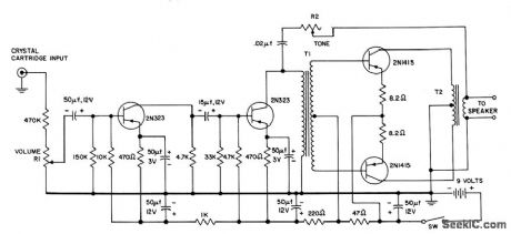
Provides 400 mw at 10% distortion. R1 is 5K audio taper and R2 is 25K linear taper- Transistor Manual, Seventh Edition, General Electric Co.,1964, p 377. (View)
View full Circuit Diagram | Comments | Reading(623)
VOLTAGE_MONITOR
Published:2009/7/14 22:34:00 Author:Jessie

Developed for use in systems having multiple DC bias voltages, to prevent damage when one supply voltage goes down while other5 remain normal. Control circuit includes its own independent AC/DC supply that ensures protection even when equipment containing RAMs and MOS devices is turned off. Failure of AC supply for monitor shuts down entire system. Can be applied to any number of supplies by adding resistive dividers, Schmitt triggers, diodes, and latches as required. Closing system power switch activates solid-state relay for applying AC line voltage to main power supplies. Half of 556 dual timer and 74LS174 hex D latch inhibit voltage monitor until all supplies have stabilized, about 500 ms later. Other half of 556 then clocks 74LS175 power-monitor latch. System then operates normally as long as all D inputs to monitor latch stay at logic 0. If one supply fails, logic 1 appears at is latch input and next clock pulse initiates shutdown of sys-tem, LED identifies supply that has failed.-J. E. Draut, Voltage Monitor Protects Against Power-Supply Failures, EDN Magazine, Nov. 20, 1977, p 239-240. (View)
View full Circuit Diagram | Comments | Reading(4082)
10_W_DIRECT_COUPLED_POWER_AMPLIFIER
Published:2009/7/14 22:34:00 Author:Jessie
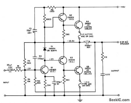


Has excellent low-frequency response, along with d-c feedback for temperature stabilization of all stages. Q2 and Q3 operate dass Bin Darlington connection to increase current gain. Fuses protect output transistorsagainst continuous sine. wave output above 10 kc. Power response at 1 w is fat from 30cps to 15 kc.- Transistor Manual, Seventh Edition, General Electric Co., 1964, p260. (View)
View full Circuit Diagram | Comments | Reading(1160)
STABILIZED_MONO
Published:2009/7/14 21:33:00 Author:May


Operates us 10:1 divider at 1,000 pps. Division ratio of mvbr remains constant for supply variations of from 40 to 400 v. Average plate voltage of V5 is adjusted automatically to maintain optimum working conditions throughout operating range.-T. Hornak, Stabilizing Monostable Multivibrators, Electronics, 33:45, p 76. (View)
View full Circuit Diagram | Comments | Reading(673)
| Pages:597/2234 At 20581582583584585586587588589590591592593594595596597598599600Under 20 |
Circuit Categories
power supply circuit
Amplifier Circuit
Basic Circuit
LED and Light Circuit
Sensor Circuit
Signal Processing
Electrical Equipment Circuit
Control Circuit
Remote Control Circuit
A/D-D/A Converter Circuit
Audio Circuit
Measuring and Test Circuit
Communication Circuit
Computer-Related Circuit
555 Circuit
Automotive Circuit
Repairing Circuit