
Circuit Diagram
Index 611
ONE_BUTTON_LATCHING_SWITCH
Published:2009/7/14 12:13:00 Author:May


The SET and RESET inputs are grounded, the inverted (-Q) output is fed back to the D input, and the pulses go into the CLOCK input. Each positive pulse makes the flip-flop toggle from one state to the other. The TLC555 chip in the ftgure serves two purposes. It inverts the pulses so that you can get a positive pulse from a switch that is connected to ground. More importantly, it also debounces the switch. When you press a button, it doesn't just make contact once-the contacts bounce, opening and closing three or four times. The 4013 would toggle once on each bounce, leading to unpredictable results. Thp TLC555 uses a resistor and capacitor to smooth out these fluctuations so that each press of the button produces only one pulse. (View)
View full Circuit Diagram | Comments | Reading(2275)
555_LATCH
Published:2009/7/14 12:10:00 Author:May
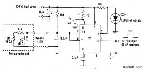
Using a 555 chip in the memory mode, this push-button-cont rolled latch switch can source up to 200 mA of load current. Only one pair of wires is required to interface the ON and OFF push buttons to the control circuitry. The memory-mode feature of the 555 chip is implemented by connecting the trigger (pin 2) and threshold (pin 6) inputs together and applying one-half the supply voltage via a resistor network. Momentarily forcing the input low causes the output to go high, while forcing the input high causes the output to go low. To facilitate remote operation of the latch switch using one pair of wires, one resistor in the voltage-divider network is installed in the remote-control unit. Shorting this resistor out with the ON push button causes the output to go high. Conversely, opening this resistor with the OFF push button induces the output to go low. The R1-C1 network connected to the RESET input (pin 4) forces the latch to come up in the OFF state when power is first applied. The LED on-off indicator is kept off whenever the discharge output (pin 7) is conducting. When the output (pin 3) goes high. (View)
View full Circuit Diagram | Comments | Reading(4343)
NONPRECISE_PHANTASTRON_VARIABLE_DELAY_2
Published:2009/7/15 2:04:00 Author:Jessie

Used to delay beginning of crt sweep for expanded display range is 5 to 175 miles. Trailing edge of screen waveform is differentiated and used to trigger blocking oscillator through trigger amplifier.-NBS, Handbook Preferred Circuits Navy Aeronautical Electronic Equipment, Vol.1.Electron Tube Circuits,1963,p N9-3 (View)
View full Circuit Diagram | Comments | Reading(498)
TUNABLE_SUBAUDIO_AMPUFIER
Published:2009/7/15 2:03:00 Author:Jessie
Commercial d-c amplifier with twin-T feedback tuningelement tunes from 0.5 to 100 cps, for analyzing low-frequency components of complexwaveforms.-J. IA. Reece, Subaudio Tunable Amplifier, Electronics, 32:45, p 72-74. (View)
View full Circuit Diagram | Comments | Reading(631)
SELF_GENERATING_FSK
Published:2009/7/15 2:03:00 Author:Jessie

Dual oscillators in Motorola MC1545G gated video amplifier are used with external frequency-determining components R1C1 and R2C2 to give 1.6 kHz for fl and 1.35 kHz for f1. Logic switching network compares output to reference and updates gate input with each cycle of output. Circuit gives smaller switching transients than are possible with separate oscillators because one oscillator is driven at frequency of the other while first oscillator is of. R3 sets transition to any level desired.- Gated Video Amplifier Applications-the MC1545, Motorola, Phoenix, AZ, 1976, AN-491, p 13. (View)
View full Circuit Diagram | Comments | Reading(692)
PULSE_WIDTH_M_O_D_U_L_A_T_O_R
Published:2009/7/15 2:03:00 Author:Jessie

Determines length of quasi-square waves used in con nection with triggering of scr's in output stage of inverter.-R. J. Kearns and J. J. Rolfe, Three-Phase Static Inverters Power Space-Vehicle Equipment, Electronics, 34:18, p 70-73. (View)
View full Circuit Diagram | Comments | Reading(867)
NONPRECISE_PHANTASTRON_VARIABLE_DELAY_1
Published:2009/7/15 2:02:00 Author:Jessie

Used to delay beginning of crt sweep for expanded display. Range is 5 to 175 miles. Trailing edge of screen waveform is differentiated and used to trigger blocking oscillator through trigger amplifier.-NBS, Handbook Preferred Circuits Navy Aeronautical Electronic Equipment, Vol. 1, Electron Tube Circuits, 1963, p N9-3. (View)
View full Circuit Diagram | Comments | Reading(577)
10_W_POWER_AMPLIFIER
Published:2009/7/15 2:02:00 Author:Jessie

Q1 provides bias current for low-power complementary-symmetry push-pull output stage Q3-Q4, which drives power transistors Q5-Q6. Q7 providesvoltage bias for Q2.-H. W. Parmer, Two Easy Ways to Stabilize Power. Transistor Hill Amplifiers, Electronics, 35:43, p 56-58. (View)
View full Circuit Diagram | Comments | Reading(0)
170_OR_850_Hz_SHlFT
Published:2009/7/15 2:01:00 Author:Jessie

Simple AF RTTY keyer uses 2N5823 silicon PNP transistor switch instead of optical coupler. Short piece of coax serves as 1-turn output link. Outer shield is grounded only at coaxial connector so braid acts as Faraday shield, eliminating capacitive signal and noise pickup from circuit.-E. Noll, Circuits and Techniques, Ham Radio, April 1976, p 40-43.
(View)
View full Circuit Diagram | Comments | Reading(1032)
DIGITAL_LATCH_WITH_SAFETY_RESET_FEATURE
Published:2009/7/14 12:08:00 Author:May

The time diagram illustrates the various modes of operation of the circuit. A high S input causes the output (Q) to go low. Thereafter, a high R input can reset Q to high, but only so long as S remains low.The asynchronous digital latching circuit is designed for use in a safety-related application, like turning off power in response to an alarm signal. During normal operation in the absence of an alarm, the SET (S) and RESET input voltages are low or off, while the output voltage (Q) is high or on. The SET input constitutes the alarm signal: Whenever S goes high (on), Q goes low (off), and thereafter remains low, even when S goes low. Thus, for example, the circuit keeps a power supply turned off even when the alarm has been shut off. If a safe condition has been restored, then the circuit can be reset to Q high by applying a high (on) signal to the RESET ( R ) input terminal. However, regardless of the R input level, Q cannot be driven high as long as S remains high; that is, the circuit cannot be reset if the alarm signal is still on. Thus, the RESET signal cannot override the alarm signal and thereby provide a false indication of safety. Also, this does not go into oscillation when the SET and RESET inputs change simultaneously.
(View)
View full Circuit Diagram | Comments | Reading(926)
DC_D_C
Published:2009/7/15 2:01:00 Author:Jessie

Line voltage is rectified, inverted at 18 kc, stepped down, and rectified to give 23 a at 6 v for thermoelectric heat-pump system.-A. L. Wennerberg and F. H. Schroedet, High-Current Converter is Small, Quiet, Low-Cost, Electronics, 37:30, p 41. (View)
View full Circuit Diagram | Comments | Reading(644)
LATCHING_SWITCH_CIRCUIT
Published:2009/7/14 12:06:00 Author:May

One button turns the LED on, the other turns it off. If you apply a positive pulse to the SET input, the output tums on. It remains on until a positive pulse is applied to the RESET input to turn it off. (TTL flip-flops such as the 74LS74 are actuated by negative, rather than positive pulses.) (View)
View full Circuit Diagram | Comments | Reading(2769)
20_VDC_FET_VOLTMETER
Published:2009/7/15 2:07:00 Author:Jessie
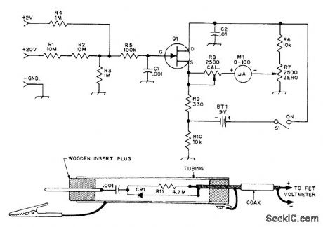
Has high input impedance as required for accurate measurements in solid-state circuit, Uses Motorola MPF102, HEP802, or equivalent N-channel JFET. If meter cannot be zeroed, change R7 to 10,000 ohms for greater zeroing range. 2-V range gives extra flexibility. Half-wave RF probe using 1N914 or equivalent high-speed switching diode responds to peak RF voltage being measured. R11 reduces peak value to RMS value. Connect probe to known 10-VRMS source, then adjust R11 so meter reads 10 V.-D, DeMaw and L. McCoy, Learning to Work with Semiconductors, QST, April 1974, p 20-25 and 41. (View)
View full Circuit Diagram | Comments | Reading(4096)
STOP_FOR_AUTOSTART
Published:2009/7/15 2:07:00 Author:Jessie
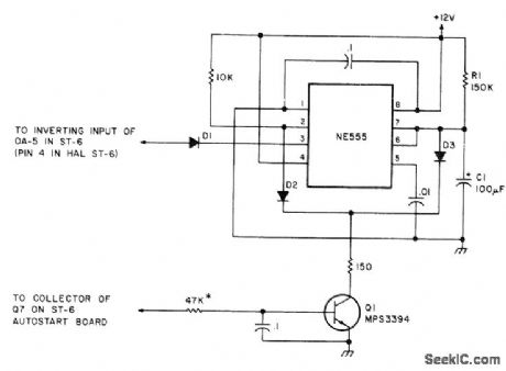
Uses 555 timer IC to make ST-6 autostart turn off motor of teleprinter if copying commercial station that does not drop its carrier when no text is being trans. mitted. Values shown for C1 and R1 give time of 15 s which, added to 25 s of ST-6 delay, gives about 40 s to turn off in presence of steady mark tone (carrier only). Useful when copying weather and press reports.-R. Bourgeois, Stop That Autostart, 73 Magazine, May 1977, p 47. (View)
View full Circuit Diagram | Comments | Reading(1297)
PB_SWITCH_ACTIVATED_LATCH
Published:2009/7/14 12:04:00 Author:May

View full Circuit Diagram | Comments | Reading(493)
SELF_EXCITED_3_PHASE_NON_PHASE_AMBIG_UOUS_BRIDGE
Published:2009/7/15 2:06:00 Author:Jessie

Each oscillating section is half-bridge converter operating in square-wave mode. Phase diagram shows derivation of synchronizing voltages.-A. G. Lloyd, Half-Bridge Inverter Provides Economical Three-Phase Power, Electronics, 34:37, p 62-65. (View)
View full Circuit Diagram | Comments | Reading(564)
TRANSPARENT_LATCH
Published:2009/7/14 12:03:00 Author:May

The circuit depicted here, which yields two independent latches per chip, is rather simple and inexpensive to build (see the figure). The second buffer A2 is wired with resistor R1 in the feedback path (ignore A1 for the moment). A2 with feedback resistor R1 is a stable latch. Because of the very low input current requirements of A2, there is hardly any voltage drop across R1. As a result, the input is the same as the output, and that is fed forward through the buffer, mA1ntA1ning a stable level. When buffer A1 is enabled, the input of A2 is driven to the same level as D. Even if A2's output (Q) is at an opposite logic level, which can happen momentarily (for a gate delay) when D is opposite to Q, Al is required to sink or source current through R1. After a gate delay, this signal propagates to Q. Both sides of R1 are now at the same logic level. When the LE signal goes inactive, A1 tristates and the latch will hold the level present at D one setup time prior to LE's going inactive. (View)
View full Circuit Diagram | Comments | Reading(1201)
O_TO_2440_MICROSEC_PHANTASTRON_DELAY
Published:2009/7/15 2:06:00 Author:Jessie

Is triggered by gating mvbr. Receives control voltage from ten-turn potentiometer calibrated in distance units. Output drives blocking oscillator through transformer. Accuracy is about 1% of delay setting.-NBS, Hand-book Preferred Circuits Navy Aeronautical Electronic Equipment, Vol. 1, Electron Tuba Circuits, 1963, p N9-2. (View)
View full Circuit Diagram | Comments | Reading(533)
PHOTOMULTIPLIER_LASER_RECEIVER_WITH_VIDEO_AMPLIFIER_
Published:2009/7/14 12:00:00 Author:May
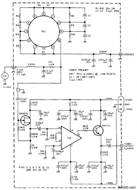
This is a circuit diagram for the inexpensive 931 side-looking PMT and its resistor divider network. This circuit maintains the proper voltages for the dynodes. The capacitors across the last three network resistors improve the frequency response of the PMT to modulated signals. A milliammeter in the PMT anode circuit registers the average PMT current under the medium to high illumination encountered during diagnostic tests. A PMT preamplifier uses a 733 (or equivalent) wideband amplifier. Because the demodulated signal can be either a direct baseband signal or a baseband signal modulated onto a subcarrier, the preamplifier must be capable of amplifying all the demodulated signal frequencies. The preamplifier is designed for a 70-Hz to 15-MHz bandwidth at the -3-dB points and for a gain of 80. Because the signal detection circuits will probably be placed in a separate housing, the video preamplifier is designed to drive a 50-Ω cable. With the high-current multiplication inherent in the PMT, the PMT noise will predominate over the video preamplifier IC noise. (View)
View full Circuit Diagram | Comments | Reading(3423)
LINE_VOLTAGE_MONITOR_1
Published:2009/7/15 2:06:00 Author:Jessie
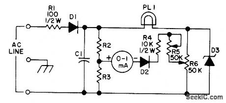
AC line voltage is rectified by D1 and filtered by C1. R2 and R3 form voltage divider that holds one meter terminal at half of rectified line voltage. DC is also applied to low-voltage calibration pot R6 through 3-W 117-V lamp or equivalent resistor PL1 which limits zener current. Any increase in line voltage increases voltage at R2-R3 junction while voltage at slider of R6 remains constant, so bridge unbalances and meter reads upscale. Zener is 70 to 100 V at 10W. R2 and R3 are equal and are from 8.2K to 15K. C1 is 50 to 100 /μF at 200 V, and diodes are power silicon with PIV above 200 and 100-mA rating.-W. P. Turner, Expanded Range Line Voltage Monitor, 73 Magazine, Jan. 1974, p 39. (View)
View full Circuit Diagram | Comments | Reading(771)
| Pages:611/2234 At 20601602603604605606607608609610611612613614615616617618619620Under 20 |
Circuit Categories
power supply circuit
Amplifier Circuit
Basic Circuit
LED and Light Circuit
Sensor Circuit
Signal Processing
Electrical Equipment Circuit
Control Circuit
Remote Control Circuit
A/D-D/A Converter Circuit
Audio Circuit
Measuring and Test Circuit
Communication Circuit
Computer-Related Circuit
555 Circuit
Automotive Circuit
Repairing Circuit