
Circuit Diagram
Index 1092
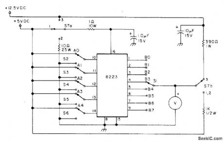
12_V_PROGRAMMER_FOR_PROM
Published:2009/7/5 20:31:00 Author:May
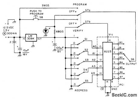
Circuit includes regulator for operation from 12-V auto storage battery. Developed to use 8223 32-word by 8-bit memory as CW identifier. All outputs of memory are initially at logic 0, so only logic 1s need to be programmed. After programming a 1, LED comes on to confirm it when S7 is switched to VERIFY. Do not hold S8 down longer than 1 s.-G. W. Kufchak, The PROM Zapper, 73 Magazine, Sept. 1976, p 112. (View)
View full Circuit Diagram | Comments | Reading(737)
HIGH_SPEED_FIFO
Published:2009/7/5 20:27:00 Author:May

Design is based on Motorola MC10143 register file, with each IC holding 8 words by 2 bits, Circuitincludes write and read enable inputs for cascading two register file packages to memory depth of 16 words. Full master-slave flip-flop operation allows simultaneous read and write. Reset is applied initially to drive both address counters to empty state.To enter data, write clock input is enabled with negative-going pulse. Write addressing is controlled by MC10178 binary counter. Used for stack registers of computing systems when register outputs are read sequentlally in sameorder that data wad entered(first-in first-out).-B.Blood, A High Speed FIFO Memory Usingthe MECL MC10143 Register Fil, Motorola,Phoenix,AZ,1974,AN-730,p 5. (View)
View full Circuit Diagram | Comments | Reading(1638)
EXCLUSIVE_OR
Published:2009/7/5 20:25:00 Author:May
gate combines both pulses at output、Values shown for R and C will double frequency of 800-μS-wide inρut pulses having repetition rate of about 130 ρer second.-K.R.Brooks,Pulse Rate Doubler Wireless World,Aρril 1976、ρ 63 (View)
View full Circuit Diagram | Comments | Reading(877)
80_W_PEP_broadband_linear_amplifier
Published:2009/7/23 22:56:00 Author:Jessie
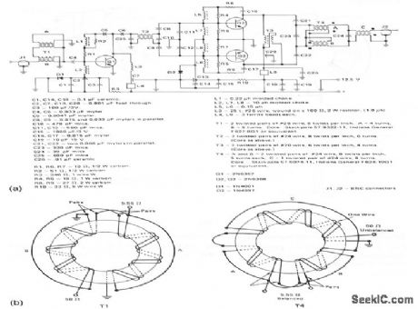
This circuit provides 80-W (PEP)into a 50-Ω load.Figure 2-51B shows the transformer details. (View)
View full Circuit Diagram | Comments | Reading(655)
LOW_CAPACITANCE_DRIVER_FOR_RAM
Published:2009/7/5 20:19:00 Author:May
Suitable for data input lines of memory system operating from 16-V supply with memory input logic swing of 16 V. Used with Motorola 1103 dynamic RAM for which transition times of data input signals should be 20 ns to give maximum memory speed. Suitable for maximum capacitances per line as high as 20 pF.-D. Brunner, A MECL 10,000 Main Frame Memory System Employing Dynamic MOS RAMs, Motorola, Phoenix, AZ, 1975, AN-583, p 13. (View)
View full Circuit Diagram | Comments | Reading(689)
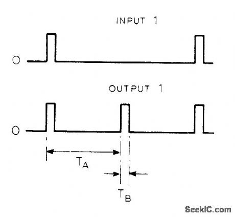
PULSE_DOUBLER
Published:2009/7/5 20:17:00 Author:May

Generates pulses at twice pulse input frequency. Input pulse at first monostable of 74123N makes it run for time TA. Negative edge, terminating TA, triggers second monostable which runs for time TB. If TAequals haff of input period and TB equals width of input pulse, desired result is aehieved wherein additional pulse is generated between input pulses. (View)
View full Circuit Diagram | Comments | Reading(1548)
H_bridge_dc_motor_controller
Published:2009/7/23 22:55:00 Author:Jessie

Figure 7-2 shows a MAX620 driving an H-bridge switch that controls the direction of a +5-Vdc motor. By toggling between the forward and reverse inputs, each driver-output pair turns on the associated pair, which passes current through the motor, causing rotation in the desired direction. To prevent all four MOSFEEs from switching on at once, update the forward/reverse inputs before clocking CE low, and do not assert forward and reverse simultaneously. Do not use a supply that will cause the gate drive to exceed the absolute maximum gate-to-source voltage of the low-side switch. MAXIM NEW RELEASES DATA Book, 1992, P. 4-27. (View)
View full Circuit Diagram | Comments | Reading(2232)
MEMORY_SAVER
Published:2009/7/5 20:16:00 Author:May

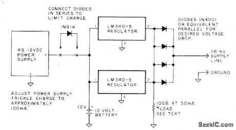
Standby battery takes over automatically during power failure to prevent memory loss. Use any rechargeable battery that can handle load. Connect one LM340-5 regulator in circuitfor each 1.2A of load current drawn by circuits to beprotected. In normal operation, output diodes are biased off by slightly higher voltage from computer. During power failure,they are switched on by removal of bias. Current is then supplied by battery. Output should be loaded with resistor drawing ahout hatf of trickle-charge current, so battery has small continuous current flow and stays charged.-C. R.Carpenter, Protect Your Memory Against Power Failure, Kilobaud, March 1978, p 73. (View)
View full Circuit Diagram | Comments | Reading(933)
Linear_regulator_with_selectable_output
Published:2009/7/23 22:55:00 Author:Jessie
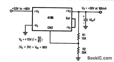
The output of this regulator can be set to any value between + 15 V and +50 V by means of voltage-divider resistors R1 and R2 (as shown by the equations). Connection information is shown in Fig. 7-3B. (View)
View full Circuit Diagram | Comments | Reading(658)
AF_MULTIPLIER
Published:2009/7/5 20:11:00 Author:May
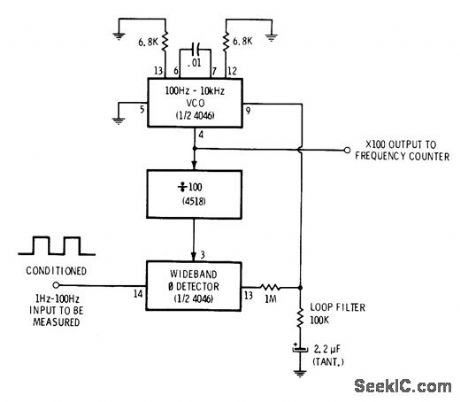
Multiplies 1-100 Hz input signal by 100 to permit measuring frequency with ordinary counter. Half of 4046 PLL is connected as 100-10,000 Hz VCO whose output is divided by 100 in 4518 dual divide-by-10 counter for comparison with input signal in other half of PLL connected as wideband phase detector.Output of detector goes to loop filter and to VCO for locking VCO at 100 times input frequency.-D. Lancaster, CMOS Cookbook, Howard W. Sams, Indianapolis, IN, 1977, p 364-366. (View)
View full Circuit Diagram | Comments | Reading(1451)
Triangle_square_wave_generator
Published:2009/7/23 22:55:00 Author:Jessie


This circuit uses two sections of 3900 op amp. The duration of the triangle-(V0) and square-wave (V02) is 1.0 mS with the values shown. Raytheon Linear Integrated Circuts, 1989, p. 4-273. (View)
View full Circuit Diagram | Comments | Reading(955)
LINEAR_RAMP_GENERATOR
Published:2009/7/23 22:55:00 Author:Jessie

Used in tester that shows computer memory performance under marginal drive currents by plotting shmoo curves. System uses two generators that differ only in component values in table. R3 in X drive circuit makes X generator lump when capacitor stops charging and starts discharging. Charging current is positive or negative depending on input voltage polarity. Npn transistors are 2N706, pnp transistors are 2N1132, and diodes are 1N921.-J. E. Gersbach, The Great Shmoo Plot: Testing Memories Automatically, Electronics, 39:15, p 127-134. (View)
View full Circuit Diagram | Comments | Reading(0)
PRF_MULTIPLIER
Published:2009/7/23 22:55:00 Author:Jessie
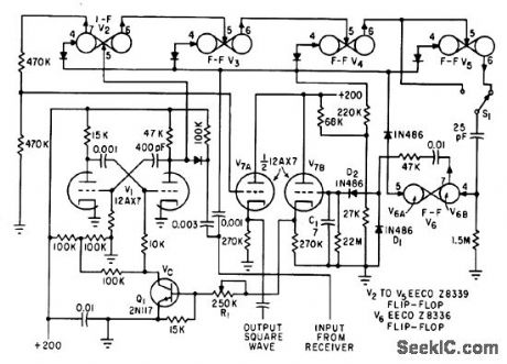
Multiplies pulse repetition frequency of ultrasonic receiver by factor of either 4 or 8, into range between 35 and 85 cps at which synchronous motors of indicalor system work best, Multiplication is based on controlled mvbr oscillator V1, whose frequency can be varied from 40 to 180 cps by varying control voltage Vc. Multiplier feedback circuit acts to control this voltage so mvbr frequency is exact multiple, 8 or 16, of input pulse rate.-H. F. Messias, Ultrasonics Measures Flow Velocity of Rivers, Electronics, 34:41, p 56-69. (View)
View full Circuit Diagram | Comments | Reading(616)
Dual_linear_regulator_with_balanced_output
Published:2009/7/23 22:55:00 Author:Jessie
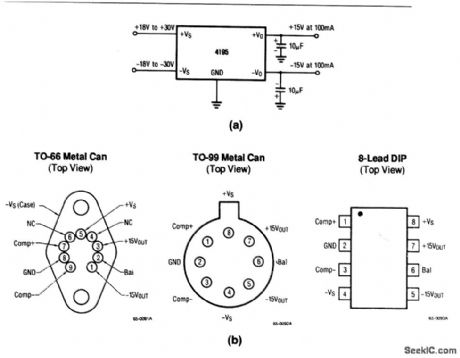
This circuit converts 18 V to +30-V input into regulated ±15-V outputs. Note that a minimum of external components (two 10-μF capacitors) are needed to complete the circuit. Figure 7-3A shows the connection information for TO-66, TO-99, and 8-lead DIP packages. (View)
View full Circuit Diagram | Comments | Reading(894)
CB_SQUELCH
Published:2009/7/23 22:52:00 Author:Jessie

Actuated by d-c limiter voltage and ac noise voltage. With no signal, out put of noise amplifier V1 is converted into positive voltage by noise rectifier of V2 and applied to grid of squelch control lube V3, making it conduct and drive grid of V4 more negative, to squelch noise.-L. G. Sands, Citizens Radio Revision Spurs Equipment Design, Electronics, 32:15, p 55-57. (View)
View full Circuit Diagram | Comments | Reading(717)
15_MINUTE_SCS_TlMER
Published:2009/7/23 22:21:00 Author:Jessie

Transistor and silicon controlled switch together serve to open relay 15 minutes after it is activated by man ual dosing of battery switch, for operating recording instruments.-T. H. Charters, Low-Cost Time Delay Controls Recorder, Electronics, 37:18, p 84. (View)
View full Circuit Diagram | Comments | Reading(601)
73333_MHz_ON_THIRD_OVERTONE
Published:2009/7/5 20:03:00 Author:May

Simple crystal oscillator circuit requires only one tripler for multiplying to 220-MHz amateur band.Mode suppression is provided by 10-μH coil which, with 4.5-pF capacitance of crystal holder, is series resonant at 24 MHz.-H. Olson, Frequency Synthesizer for 220 MHz, Ham Radio, Dec. 1974, p 8-14. (View)
View full Circuit Diagram | Comments | Reading(1056)
Negative_variable_voltage_reference_VSUBOUT_SUB_is_higher_than_reference_zener
Published:2009/7/23 22:21:00 Author:Jessie

This circuit is similar to that of Fig. 10-45, except that a variable negative-voltage reference is provided at VOUT (View)
View full Circuit Diagram | Comments | Reading(773)
16_channel_sequential_differential_mux_demux
Published:2009/7/23 22:19:00 Author:Jessie

Figures 2-18 and 2-19 show a typical application circuit and pin configurations, respectively, for the MAX7506/07. This circuit is similar to that shown in Fig. 2-17, but with 16-channel operation. MAXIM HIGH-RELIABILITY DATA Book, 1993, P. 1-49. (View)
View full Circuit Diagram | Comments | Reading(716)
DOUBLER_FOR_TACHOMETER
Published:2009/7/5 19:58:00 Author:May

Frequency of input from tachometer is doubled by charging and discharging of C1 to reduce ripplein DC output voltage of tachometer circuit. Opamp 2 provides bias current for opamp 1, while Q1 drives large load currents and provides DC level shift required for bringing output voltage to zero when input frequency is zero.-T. Frederiksen, Frequency-Doubling Tach Operates from a Single Supply,EDN Magazine, June 5, 1977, p 208. (View)
View full Circuit Diagram | Comments | Reading(1563)
| Pages:1092/2234 At 2010811082108310841085108610871088108910901091109210931094109510961097109810991100Under 20 |
Circuit Categories
power supply circuit
Amplifier Circuit
Basic Circuit
LED and Light Circuit
Sensor Circuit
Signal Processing
Electrical Equipment Circuit
Control Circuit
Remote Control Circuit
A/D-D/A Converter Circuit
Audio Circuit
Measuring and Test Circuit
Communication Circuit
Computer-Related Circuit
555 Circuit
Automotive Circuit
Repairing Circuit