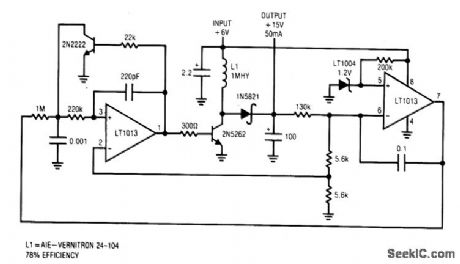
Circuit Diagram
Index 1099
Signal_line_circuit_protectors_fault_protected_switches
Published:2009/7/23 22:28:00 Author:Jessie


Figures 2-34 and 2-35 show a typical application circuit and pin configuration, respectively, for the MAX366. Pin configurations for the MAX337 are shown in Fig.2-36. These ICs are multiple, two-terminal circuit protectors. Placed in series with signal lines, each two-terminal device protects sensitive circuit components from damaging voltage near and beyond the normal supply range. The ICs are used at interfaces where sensitive circuits connect to the external world, and potentially damaging voltage (up to 135 V beyond the supply rails) might be encountered during power-up, power-down, or fault conditions. The ICs can be used to protect either analog or digital signals using unipolar (5 V to 44 V) or bipolar (±5 V to±22 V) supplies. The ICs are essentially fault-protected switches that are always on when power is applied. On resistance is 100Ω (max.), and leakage is less than 1nA at +25℃. When signal voltages exceed, or are within 1.5 V of the supply voltages, or when power, is off, the two-terminal resistance increases and becomes a virtual open circuit. This ensures low current during fault conditions. The protected side of the switch maintains the correct polarity and clamps about 1.5 V below the supply rail. There are no glitches or polarity reversals going into or coming out of a fault condition. ESD (electrostatic discharge) protection is greater than 2 kV.MAXIM NEW RELEASES DATA Book, 1995, P. 1-109, 1-110. (View)
View full Circuit Diagram | Comments | Reading(824)
PLL_IF_AND_DEMODULATOR
Published:2009/7/3 4:40:00 Author:May
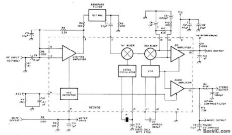
Signetics NE563B IC(In dashed lin es)serves as completeIF amplifier and demodulator for FM broadcastrecelver, Circuit uses downconversion from 10.7 MHz to 900 kHz, where phase detector operates. Ceramic bandpass filter provides IF selectivity at 10.7 MHz. X1 can be 9.8-MHz ceramic resonator, LC network, crystal, or capacitor.-H. Olson, FM Detectors, Ham Radio, June 1976, p22-29. (View)
View full Circuit Diagram | Comments | Reading(1790)
ADAPTIVE_REFRESH
Published:2009/7/3 4:36:00 Author:May
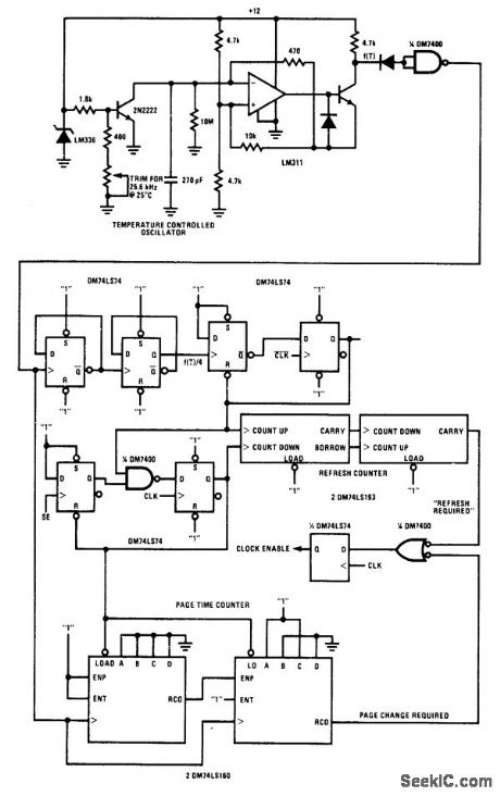
Circuit monitors system utilization of National MM2464 64-kilobit charge-coupled device (CCD). Refresh time and maximum page times are determined by two counters that obtain clock signals from temperature-controlled oscillator.- Memory Applications Handbook, National Semiconductor, Santa Clara, CA, 1978, p 7-1-7-10. (View)
View full Circuit Diagram | Comments | Reading(650)
195_KC_SONAR_F_M_DEMODULATOR
Published:2009/7/23 22:28:00 Author:Jessie
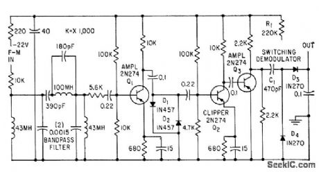
Used in playback of active sonar f-m signals multiplexed onto one track of magnetic tape, for training students at land-based sonar. Bandpass fiber at input demodulator selects band of frequencies associated with desired f-m terrier. Output from filter is amplified and dipped for switching demodulator, whose output is varying component of average modulating signal current.-M. H. Damon, Jr., Tape Target Classifier Trains Sonar Operators, Electronics, 33:13, p 65-69. (View)
View full Circuit Diagram | Comments | Reading(650)
Basic_step_up_voltage_regulator
Published:2009/7/23 22:28:00 Author:Jessie
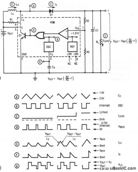

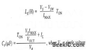
Figures 4-2A and 4-2B show a basic step-up voltage regulator, and waveforms, respectively. Component values are tailored to circuit requirements, as follows:
where: IA feedback divider current (typically 50 to 100 μA)where: Vs =supply voltage, VD= diode forward voltage, IL= dc load current, VSW= sauration voltage of Q 1 (typical 0.5 V), If IMAX is more than 375 mA, Q1 must be replaced with a power transistor.
(View)
View full Circuit Diagram | Comments | Reading(734)
SUMMING_AMPLIFIER
Published:2009/7/3 4:34:00 Author:May
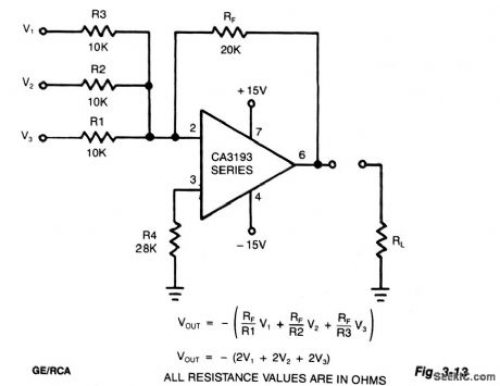
This circuit uses a CA3193 BiMOS op amp.Because mput nolse of the amplifier is increased by RF/R1//R2//R3,nd the gam that a single input will amplify is the gam of only one of the input channels (RF/R1),for good noise performance,use the smallest number of inputs. (View)
View full Circuit Diagram | Comments | Reading(0)
Simple_RS_232_receiver
Published:2009/7/23 22:27:00 Author:Jessie
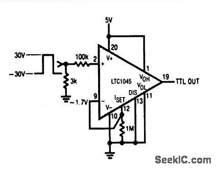
This circuit shows a simple way to build a battery-powered RS-232 receiver. The input voltage can be driven as much as ±30 V without adverse effects because the 100-kΩ resistor prevents device damage. With a 1-MΩ RSET resistor at pin 12, the LTC1045 draws only 100 μA of quiescent current, and has a propagation delay of 1.2 μs. Only a single 5-V supply is required. (View)
View full Circuit Diagram | Comments | Reading(708)
POLARITY_REVERSING_LOW_POWER_AMPLIFIER
Published:2009/7/3 4:33:00 Author:May
View full Circuit Diagram | Comments | Reading(490)
QUADRATURE_DEMODULATOR
Published:2009/7/3 4:32:00 Author:May
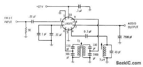
Quadrature coil associated with balanced-mixer demodulation system is connected to pin 6 of National LM373 IC, and output signal is taken from pin 7.Good output is obtained with only ±5 kHz deviation at either 455 kHz or 10.7 MHz. Can be operated as wideband or narrow-band circuit by choosing appropriate interstage and output LC and RC components.-E. M. Noll, Linear IC Principles, Experiments, and Projects, Howard W. Sams, Indianapolis, IN, 1974, p 350-351. (View)
View full Circuit Diagram | Comments | Reading(1665)
FET_SUPPLIES_CONSTANT_CURRENT
Published:2009/7/23 22:27:00 Author:Jessie
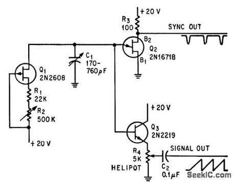
Utilizes near-zero temperature drift of fet at bias point, to make performance independent of battery or line voltage fluctuations.-E. Elad, FET Insures Stable Sawtooth Wave, Electronics, 39:16, p 122-123. (View)
View full Circuit Diagram | Comments | Reading(570)
WAVE_SYNTHESlZER
Published:2009/7/3 4:31:00 Author:May
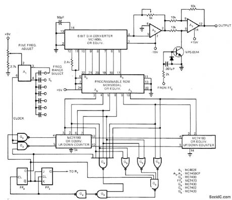
Virtually any symmetrical waveform can be generated by using only IC counters, a read-only memory, and a monolithic D/A converter. Only first 90 °of waveform need be digitized; this information can be manipulated to generate other 270 °and repeated as often as necessary. To digitize desired wave form, divide first 9O °into 64 points, calculate sine or other function for each, multiply each result by 63 to normalize, round off, convert each to 6-bit binary equivalent, take complements, and use results for programming ROM.Article describes operation of circuit in detail.Use of MC1480 8-b'ffi monolithic D/A converter gives better resolution than is possible with MC1406L 6-bit D/A converter because 8-bit words give 256 discrete output levels instead of 64.-K. Huehne, Programmable ROMs Offer a Digital Approach to Waveform Synthesis, EDN Magazine, Aug. 1, 1972. p 38-41. (View)
View full Circuit Diagram | Comments | Reading(596)
High_input_impedance_instrumentation_amplifier
Published:2009/7/23 22:27:00 Author:Jessie
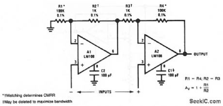
Compare this circuit to that of Fig,10-38 and 10-49. (View)
View full Circuit Diagram | Comments | Reading(0)
WIDE_BAND_AGC_AMPLIFIER
Published:2009/7/3 4:31:00 Author:May

The NE592 is connected in conjunction with a MC1496 balanced modulator to form an excellent auto-matic gain control system. The signal is fed to the signal input of the MC1496 and rc-coupled to the NE592. Unbalancing the carrier input of the MC1496 causes the signal to pass through unattenuated. Rec-tifying and filtering one of the NE592 outputs produces a dc signal which is proportional to the ac signal amplitude. After ftltering, this control signal is applied to the MC1496, causing its gain to change. (View)
View full Circuit Diagram | Comments | Reading(4611)
LINEAR_BOOTSTRAP
Published:2009/7/23 22:27:00 Author:Jessie

Charging current of C1 is kept constant, resulting in high linearity of ramp output. Positive-going square wave is on collector of Q8 while ramp is being generated.-D. A Williams Jr., Transistors Ruggedize Airborne Telemetry Keyer, Electronics, 31:37, p 81-83. (View)
View full Circuit Diagram | Comments | Reading(778)
STEP_UP_SWITCHING_REGULATOR_FOR_6_V_BATTERY
Published:2009/7/3 4:27:00 Author:May
View full Circuit Diagram | Comments | Reading(781)
Isolated_data_acquisition_system
Published:2009/7/23 22:27:00 Author:Jessie

This circuit shows an 8-input LTC1090 data-acquisition IC connected to a system with 500-V isolation (provided by 4N28 opto-isolators). The number of channels can be increased to 16, 24, 32, etc, with one additional opto-isolator used to increase the number of channels in multiples of 8. Up to 24 channels can be powered directly by the LT1021. The circuit is capable of transferring serial data at about a 15-kHz rate. A code written for the Motorola 68HC05 processor is available from Linear Technology. (View)
View full Circuit Diagram | Comments | Reading(1961)
SIGLE_TUNED_DETECTOR
Published:2009/7/3 4:27:00 Author:May

RCA CA3089E IC serves as communication receiver subsystem providing three-stage FM IF amplifier/limiter channel, with signal-level detectors for each stage, and quadrature detector that can be used with single-tuned detector coil. Detector also supplies drive to AFC amplifier whose output can be used to hold local oscillator orl correct frequency. Level-detector stages supply signal for tuning meter. Values shown are for 10.7-MHz IF.-E. M. Noll, Linear IC Principles, Experiments, and Projects, Howard W. Sams, Indianapolis, IN, 1974, P 374-379 (View)
View full Circuit Diagram | Comments | Reading(1641)
UJT_TIMER
Published:2009/7/23 22:26:00 Author:Jessie

Charging current of C1 should be greater than 2Gmicroamp peak-point current at which Q3 is triggered and less thon 8-ma sustaining current of Q3, so ujt will turn off after it is triggered. 2N2422A may be used for Q3.-A. A. Lampell, Off-the-Shelf Integrated Circuits for Versatile and Accurato Timer, Electronics, 38:25, p 70-73. (View)
View full Circuit Diagram | Comments | Reading(696)
A_LITHIUM_BATTERY’S_STATE_OF_CHARGE_INDICATOR
Published:2009/7/3 4:26:00 Author:May

State-ofiCharge indication of a sloping-voltage discharge can be used as a state-of-charge indicator. A typical voltage comparator circuit that gives a visual indication of state-of-charge is shown. Components identified are for a 4-cell input voltage of 9.6 to 5.2 volts. (View)
View full Circuit Diagram | Comments | Reading(1081)
Double-barreled double-block circuit diagram
Published:2011/8/1 21:20:00 Author:Ecco | Keyword: Double-barreled , double-block
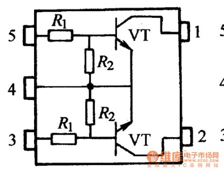
The main transistor with resistance is a kind of small power tube, which is used as the electronic switch or inverter in household appliances and other electronic devices. Some band-stop tubes contain two transistors and lead 5-6 feet (dual-barreled dual-resistance model, it is shown in Figure)
(View)
View full Circuit Diagram | Comments | Reading(450)
| Pages:1099/2234 At 2010811082108310841085108610871088108910901091109210931094109510961097109810991100Under 20 |
Circuit Categories
power supply circuit
Amplifier Circuit
Basic Circuit
LED and Light Circuit
Sensor Circuit
Signal Processing
Electrical Equipment Circuit
Control Circuit
Remote Control Circuit
A/D-D/A Converter Circuit
Audio Circuit
Measuring and Test Circuit
Communication Circuit
Computer-Related Circuit
555 Circuit
Automotive Circuit
Repairing Circuit

