
Circuit Diagram
Index 1093
SINE_WAVE_DOUBLE_
Published:2009/7/5 19:51:00 Author:May

Frequency of sinusoidal input signal VS is doubled to give sine-wave output with total harmonic distortion less than 0.6%,With input of 4 V P-P at 10 kHz、output is1V P-P at 20 kHz. X and Υ offset adjustments are nulled to minimize harmonic content of out-put.-″PhaseˉLocked Loop Data Book,''Exarlntegrated Systems,Sunnyvale,CA,1978,p 9-16. (View)
View full Circuit Diagram | Comments | Reading(729)
FET_DOUBLE
Published:2009/7/5 19:40:00 Author:May

Siliconix E300 matched FETs are connected as common-gateamplifiers in blanced push-push circuit giving up to 100% efficiency as frequency multiplier in UHF range.series-tuned output trap L2C8 increase rejecttion of third-orde harmonics to greater than 70dB.Positive bias of 0.5 V is applied to FET gates to permit inclusion of balance control R2,Gainof doubler is about 1 dB.-''Analog Switches ''and Their Applications,''Siliconix、Santa Clara,CA、1976 p7-52 (View)
View full Circuit Diagram | Comments | Reading(1236)
SQUARE_WAVE_DOUBLER
Published:2009/7/5 19:18:00 Author:May
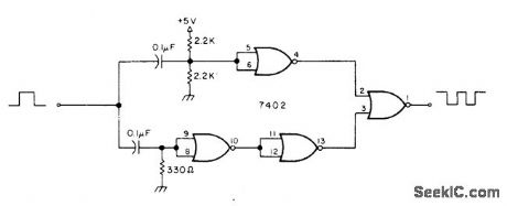
Circuh locks onto both rse and fall of input square wave, to give identical square-wave output at doubled frequency. For high input frequencies, use smaller capacitance values.-Circuits, 73 Magazine, April 1977, p 164. (View)
View full Circuit Diagram | Comments | Reading(1943)
MULTIPLIER_DIVIDER
Published:2009/7/5 19:13:00 Author:May
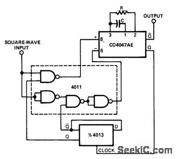
Choice of values for R and C determines multiplication or division factor acting on square-wave input frequency. 0utput of 4013 flip-flop sets gates of 4011 to steer input clock pulse of RCA CD4047AE mono MVBR to proper inputs. When rising edge of input triggers mono, Q output of mono goes high and switches flip-flop, preparing mono to accept falling-edge trigger. Since 4047 locks out inputs until ittimes out, mono triggers only on first falling edge occurring after its output goes low. Mono pulse length is about 2.5RC. With 60-Hz input clock, mono pulse length less than 8.33 ms allows triggering on every transition, to give 120-Hz output.-P. A. Lawless, One-Shot Forms Frequency Multiplier, EDN Magazine, Aug. 5, 1978, p 72. (View)
View full Circuit Diagram | Comments | Reading(1449)
PLL_MULTIPLIES_BY_10
Published:2009/7/5 3:55:00 Author:May

Used with frequency counter to measure very low frequencies. Two such circuits can be cascaded to give multiplication by 100. Requires +5 V and +12 V supplies.-H. S. Laidman, Upgrading Inexpensive Counters, CQ, Aug. 1975, p 16-22. (View)
View full Circuit Diagram | Comments | Reading(622)
WIDEBAND_DOUBLER
Published:2009/7/5 3:46:00 Author:May
AC-coupled multiplier block is connected in squaring mode to provide second harmonic of input frequency with no tuned circuits. Circuit operates over wide bandwidths without adjustment. Output is low-distortion sine wave; total harmonic distortion is typically 1%. Output can be taken from pin 2 or 14, depending on phase desired. Circuit will work with R7 grounded, but offset adjustment can be used to minimize distortion. Maximum operating frequency is several megahertz.-W.G. Jung, IC Op-Amp Cookbook, Howard W.Sams, Indianapolis, IN, 1974, p 258-259. (View)
View full Circuit Diagram | Comments | Reading(592)
PUSH_PUSH_DOUBLER
Published:2009/7/5 3:39:00 Author:May
Usefui in VF0 output circuits where oscillator operates at half output frequency of doubler. Circuit helps reduce osdllator instability during load changes while having about same efficieney as straight amplifier. Uses two sections of RCA CA3028A differential amplifier as doubler (U1C is not used).Values of tuned circuit depend on frequency, which can be up to 120 MHz.-D. DeMaw, Understanding Linear ICs, QST, Feb. 1977,p 19-23. (View)
View full Circuit Diagram | Comments | Reading(643)
500_5000_Hz_SQUARE_WAVE_DOUBLER
Published:2009/7/4 22:27:00 Author:May

Circuit shows virtually no deviation from 50% duty cycle over entire frequency range. Four NOR gates in CD4001AE IC form edge detector that presents negative pulse to 555 IC timer on both rising and falling edges of input square wave, to achieve frequency doubling. High-gain 741 opamp amplifies any difference between DC level at timer outputand reference equal to half of supply voltage, to send correction voltage to pin 5 of timer for forcing output to 50% duty cycle.-L. P. Kahhan, Frequency Doubler 0utputs Square Wave with 50% Duty Cycle, EDN Magazine, June 5, 1977, p 211-212. (View)
View full Circuit Diagram | Comments | Reading(1903)
PROGRAMMABLE_PLL_SYNTHESIZE_MULTI_PLIE
Published:2009/7/4 22:14:00 Author:May

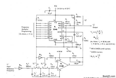
Uses programmable timer/counter A 1 as vco for generating frequencies both aboveand below that of square-wave reference Phase-Locked output frequency is not direct multiple of reference frequency. 2240 can lock on programmable multiple or on subharmonic reference. For values shown, phase-locked loop is locked through common frequency submultiple of 10 Hz, to give sampling rate of 10 Hz for reference input.-W. G. Jung, IC Timer Cookbook, Howard W. Sams, Indianapolis, IN, 1977, p 220-224. (View)
View full Circuit Diagram | Comments | Reading(566)
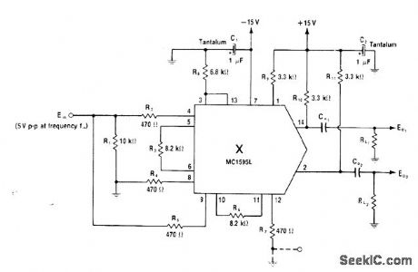
BROADBAND_LOW_FREQUENCY_DOUBLER
Published:2009/7/4 22:05:00 Author:May

Motorola MC1596G balanced modulator functions as frequency doubler when same signalis injected into both input ρorts (plns 1 and 8),Doubling occurs audio range and up to about 1 MHz.-R.Hejhall,″MC1596 Balanced Modulator,″Motorola,Phoenix、AZ,1975,AN-531,p 10 (View)
View full Circuit Diagram | Comments | Reading(958)
245_MHz_TO_147_MHz
Published:2009/7/4 21:56:00 Author:May
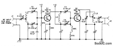
UsesQ1 as tripler to73.5 MHz for frequency-modulated input of 24.5MHz, and Q2 as doubler whose output tank is tuned to 147 MHz by C6 and L3. Output is about 200 mW of RF. L1 is 20 turns No. 26 with center tap, on 0.5-cm form. L2 is 8 turns No. 22 on 0.8-cm form. RFC is 25 turns on 0.5-cm form. Article covers troubles likely to be encountered.-B.Hoisington, Frequency Multiplication the Easy Way, 73 Magazine, Oct. 1973, p 69-71. (View)
View full Circuit Diagram | Comments | Reading(594)
DOUBLING_150_MHz
Published:2009/7/4 21:43:00 Author:May
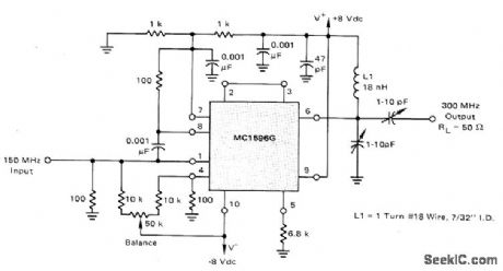
Motorola MC1596G balanced modulator is connected for doubling at RF and UHF.With output filtering shown,all spurious outputs are at least 20 dB below desired 300-MHz output. Suppression of spurious outputs is poorer for higher input frequencies,being only 7 dB down for 400-MHz output, but performance is still superior to that of conventional transistor doubler.-R. Hejhall, MC1596 Balanced Modulator, Motorola, Phoenix, AZ, 1975, AN-531, p 10. (View)
View full Circuit Diagram | Comments | Reading(539)
DOUBLING_200_MHz
Published:2009/7/4 21:30:00 Author:May
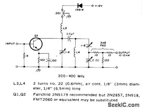
Recommended for use with VHF/UHF converters having inptuts of 180 to 220 MHz, with 5-10 mW output. Diode in series with power supply prevents damage if polarity is reversed.-J. Reisert, VHF/UHF Techniques, Ham Radio, March 1976, p 44-48. (View)
View full Circuit Diagram | Comments | Reading(1019)
SONAR_BEARING_INDICATOR
Published:2009/7/23 22:18:00 Author:Jessie
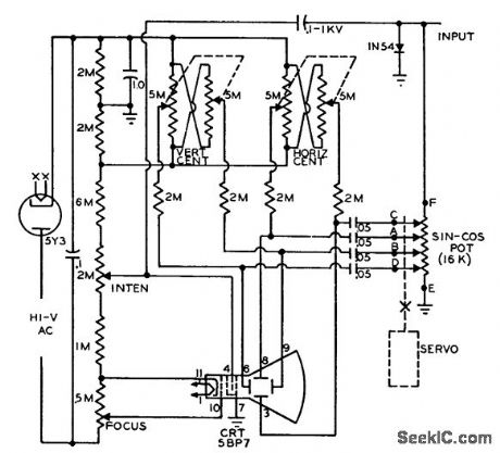
Visual indicator using ordinary cro can be synchronized with rotating directional underwater acoustic transducer, to indicate relative bearing of arriving signal from target. Transducer synchro output, proportional to bearing, drives small servo motor having standard 4-fop sine-cosine potentiometer. Detector output is applied across pot, and four vector outputs are fed to cathode-ray deflection plates. A-c voltage produces rotating bar, and diode clipping of half the signal converts bar to pointer emanating from center of screen. With target signal present, input amplitude is adjusted to produce line from center to edge of screen.-Target Bearing Indicator, Electronic Circuit Design Handbook, Mactier Pub. Corp., N.Y., 1965, p 123. (View)
View full Circuit Diagram | Comments | Reading(657)
MULTIPLES_OF_25_MHz
Published:2009/7/4 21:19:00 Author:May
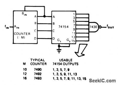
Three TTL circuits provide integral frequency-multiplication ratiosbetween1 and 8. BCD outputs of counter having modulus M are fed to inputs of 74154 4-line to16-line decoder.As outputs of counter change、at rate equal to input frequency divided by counter modulus M,each goes low at samerate Output of NAND gatethus goes high oncefor each input to gate from decoder.If 7490 decade counter is used and inputis 1 MHz,BCD outputs of 7490limit usable outputs of 74154 to lines 1,3,5,7,and 9.Since inputs to 74154 change at l00-kHz rate,output from gate will be n×100 kHz .With inρut of 25 MHz、output is integral multiple of 2.5MHz.-R .s Stein,Three TTLIC's Provide Frequency Multiplication,EON Magazine,April 5、1975、p 117 and 119. (View)
View full Circuit Diagram | Comments | Reading(1493)
SQUARER
Published:2009/7/4 21:04:00 Author:May


Simple tunnel-diode circuit doubles frequency efficiently without use of tuned circuits. Fundamental and other harmonics of input areat least 30 dB below level of frequencydoubled output. Circuit operates from DC to upper frequency limit of opamp used. Adjust R2 so diode current is at peak of its bias current, to eliminate offset at amplifier output.-R. Kincaid, Squaring Circuit Makes Efficient Frequency Doubler, EDN/EEE Magazine, Aug. 15, 1971,p 45. (View)
View full Circuit Diagram | Comments | Reading(803)
Complete_three_chip_AM_radio_station
Published:2009/7/23 22:18:00 Author:Jessie

This circuit is a complete microphone-to-an tenna AM radio station, producing a stable 1-Vpp 1-MHz signal at the antenna. Construction and operation of this circuit might require FCC review and/or licensing. The carrier is generated by A1, connected as a quartz-stabilized oscillator, similar to that of Fig. 5-18. The A1 output is applied to modulated RF power-output stage A2. Microphone amplifier A3 supplies bias to pins 1 and 8 of A2, resulting in an amplitude-modulated RF carrier at the A2 output. The circuit is calibrated by adjusting the 50-Ω oscillator potentiometer for a stable 1-Vpp 1-MHz signal at the A1 output. (View)
View full Circuit Diagram | Comments | Reading(632)
8_channel_sequential_differential_mux_demux
Published:2009/7/23 22:18:00 Author:Jessie

Figures 2-16 and 2-17 show a typical application circuit and pin configurations, respectively, for the MAX7501/02/03. In this circuit, the IC acts as a multiplexer or demultiplexer by inter-changing the analog inputs and outputs. Each channel is sampled in sequence by signals from a DM7493 under the control of an external clock. MAXIM HIGH-RELIABILITY DATA Book, 1993, P.1-47. (View)
View full Circuit Diagram | Comments | Reading(1558)
Photovoltaic_cell_amplifier
Published:2009/7/23 22:18:00 Author:Jessie
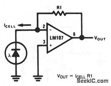
As shown by the equation, VOUT depends on photovolataic-cell current and R1 (which should be chose for or scale factor) (View)
View full Circuit Diagram | Comments | Reading(782)
HYBRID_SILICON_BOXCAR
Published:2009/7/23 22:18:00 Author:Jessie
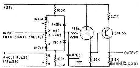
Signal-to-noise ratio of silicon hybrid is up to 2 db better than germanium at all temperatures. Only one transistor is needed for high-temperature stability. Input to boxcar should be from 150-ohm source.-A. G. Lloyd, Half-Bridge Inverter Provides Economical Three-Phase Power, Electronics, 34:37, p 62-65. (View)
View full Circuit Diagram | Comments | Reading(487)
| Pages:1093/2234 At 2010811082108310841085108610871088108910901091109210931094109510961097109810991100Under 20 |
Circuit Categories
power supply circuit
Amplifier Circuit
Basic Circuit
LED and Light Circuit
Sensor Circuit
Signal Processing
Electrical Equipment Circuit
Control Circuit
Remote Control Circuit
A/D-D/A Converter Circuit
Audio Circuit
Measuring and Test Circuit
Communication Circuit
Computer-Related Circuit
555 Circuit
Automotive Circuit
Repairing Circuit