
Circuit Diagram
Index 1086
41_5050_60AND_60_71_MHz
Published:2009/7/5 21:51:00 Author:May

Three Indopendent low-noise VCOs are usedin 41-71 MHz frequency synthesizer, Control voltage is obtained from phase-comparator output of synthesizer. Outputs are chosen by selector switch.Texas Instruments SN72733 wideband amplifier is used for decoupling. Cascade arrangement provides two independent outputs at low impedance.-U. L. Rohde, Modem Design of Frequency Synthesizers, Ham Radio, July 1976, p 10-23. (View)
View full Circuit Diagram | Comments | Reading(1077)
THREE_PHASE_POWER_FACTOR_CONTROLLER
Published:2009/7/5 21:51:00 Author:May

The modified power-factor controller, developed at the Marshall Space Flight Center, employs a phase detector for each of the three phase windings of a delta-connected induction motor. The phase-difference sum is the basis for control. Instabilities of earlier systems are overcome with improved feedback control incorporating a 20Hz bandwidth signal. (View)
View full Circuit Diagram | Comments | Reading(3210)
CURSOR_CONTROL
Published:2009/7/5 21:49:00 Author:May

Full software cursor control permits writing anywhere on screen without restrictive top-to-bottom/left-to-right format. System uses 18 of possible 32 ASCII control codes in TV IIsystem having 8K BASIC.Three 7445 BCD-to-decimal decoders operate in 3-line-to-S-line mode wherein pin 12 becomes chip enable. When pin 12 goes low, one of the eight outputs will go low.-R,wright.Utilize ASCII Control Codes!,Kilobaud,Oct.1977,p80-83 (View)
View full Circuit Diagram | Comments | Reading(1551)
400_Hz_SERVO_AMPLIFIER
Published:2009/7/5 21:47:00 Author:May
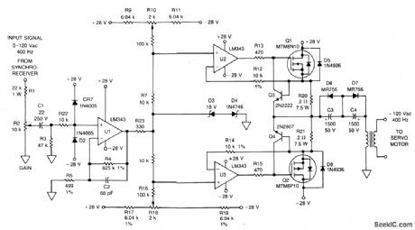
The signal from a synchro receiver or a variable resistive cam follower (potentiometer) is boosted by operational amplifier U1, whose output swing is limited by back-to-back zeners D3 and D4. The signal is then applied to operational amplifiers U2 and U3, which drive the gates of Q1 and Q2 respectively. The npn transistor (Q3) is a fast current limiter for the n-channel MTM8N10; a pnp transistor (Q4) performs the same function for the p-channel MTM8P10. Capacitors C3 and C4 eliminate the need for accurate dc offset zeroing. T1 steps up the output voltage to 120 V for the 400 Hz servo motor. (View)
View full Circuit Diagram | Comments | Reading(1987)
_ADDRESS_STATE_ANALYZER
Published:2009/7/5 21:44:00 Author:May
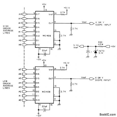
Dynamic fluctuations of 16-bit memory address bus are dis played on CRO for troubleshooting. Two MC1408 8-bit DACs drive inputs of CRO with analog equivalents of eight high-order and eight low-order address lines. Display serves as visual picture of computer in action, in which accessing of unexpected memory locations is instantly visible. Incoming address lines can be connected to MC1408s in any order. Article covers evaluation of scope patterns.-S. Ciarcia, A Penny Pinching Address State Analyzer, BYTE, Feb. 1978, p 6, 8, 10, and 12. (View)
View full Circuit Diagram | Comments | Reading(736)
HIGH_VOLTAGE_SUPPLY
Published:2009/7/5 21:44:00 Author:May

Circuit NotesA 6 V battery can provide 100-150 Vdc center-tapped at a high internal impedance (not dangerous though it can inflict an unpleasant jolt). A 6.3 V transformer is connected in reverse with a transistor used in a Hartley oscillator configuration. The frequency of operation may be controlled by varying the value of the 10 K ohm resistor. The 10 μF capacitor must have a working voltage of at least 250 Vdc. (View)
View full Circuit Diagram | Comments | Reading(0)
DC_SERVO_DRIVE_EMPLOYS_BIPOLAR_CONTROL_INPUT
Published:2009/7/5 21:41:00 Author:May
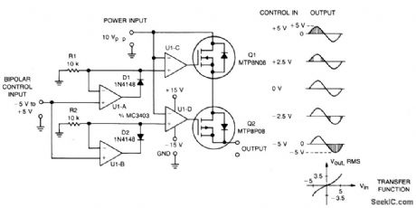
This circuit accepts bipolar control inputs of ±5 V and provides a phase-chopped output to a dc load (such as a servo motor) of the same polarity as the input. The rms voltage of the output is closely proportional to the control input voltage.
N-channel and p-channel TMOS devices, Q1 and Q2, are connected in anti-series to form a bidirectional switch through which current can flow in either the forward or reverse direction. Control circuits turn Q1 and Q2 on when they are reverse biased, bypassing their reverse rectif er and increasing circuit efflciency. Each device is allowed to turn off only when forward biased.
The Q1-Q2 switch connects the ac power source to the load when its instantaneous voltage is the same polarity and less than the control voltage. U1a is conftgured as an ideal positive rectifter whose output follows the control voltage when it is positive, and is zero otherwise. Similarly, U1b is a negative rectifier. U1c tums Q1 on whenever the ac input voltage is lower than the positive rectifier output. For negative control voltages, Q1 is turned on only during the negative half-cycle. For positive control voltages, Q1 is tumed on during the end portions of the positive half-cycle. Similarly, U1d turns Q2 on whenever the ac input voltage is higher than the output of the negative rectifier. (View)
View full Circuit Diagram | Comments | Reading(911)
38_kHz
Published:2009/7/5 21:40:00 Author:May

Simple opamp circuit provides convenient sine-wave AF signal.-J. s. Lucas. Unusual Sinewave Generator.Wireless World. May 1977.p 81 (View)
View full Circuit Diagram | Comments | Reading(2774)
OSCILLATOR_CONTROL
Published:2009/7/5 21:39:00 Author:May

Digital inputs from mioroprocessor to Precision Monolithics DAC-76CX 8-bit companding D/A converter provide 8159:1 frequency range for AF oscillator, from 2.5 to 20,000 Hz. DAC functions as programmable current source that altemately charges and dischatges capacitor between precisely controlled upper and lower limits. Since both limits are derived by dividing power supply volt ages, frequency is independent of changes in supply voltage.Design equations are gtven.-D.Soderquist, Exponential Digitally Controlled Oscillator Using DAC-76, Precision Monolithics, Santa Clara, CA, 1977, AN-20, p 1. (View)
View full Circuit Diagram | Comments | Reading(986)
FET_TIMER
Published:2009/7/23 22:15:00 Author:Jessie
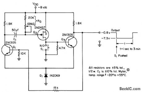
Darlington-like pair Q2-Q3 serve with Q1 as monostable mvbr, most useful as timer because high input impedance allows use of modest capacitors to obtain long time delays. In stable state, Q2 is on and Q3 is saturated, holding Q1 off.-L. J. Sevin, Jr. Field-Effect Transistors, McGraw-Hill, N.Y., 1965, p 89. (View)
View full Circuit Diagram | Comments | Reading(783)
HIGH_VOLTAGE_GEIGER_COUNTER_SUPPL
Published:2009/7/5 21:38:00 Author:May
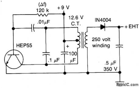
Circuit NotesThis circuit will generate about 300 volts dc-at a very low current,but enough for a GMtube. (View)
View full Circuit Diagram | Comments | Reading(0)
VSUBPP_SUB_handshake_circuit
Published:2009/7/23 22:11:00 Author:Jessie
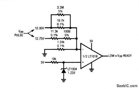
This circuit verifies that the VPP pulse generators (Figs. 6-49 and 6-50) are producing the correct output before pulsing begins. This is done by comparing the VPP output against the LT1004 reference. The LT1016 output goes low if the VPP output is correct. The resistor values shown allow for possible variations in VPP voltage because of component-tolerance stack-up. The output of the VPP generator should be set within 0.4% of nominal value when using this circuit. This can be done by trimming, or using 0.05% resistors in place of the 0.1% units specified. (View)
View full Circuit Diagram | Comments | Reading(605)
VOLTAGE_CONTROLLED_ATTENUATOR
Published:2009/7/5 21:37:00 Author:May
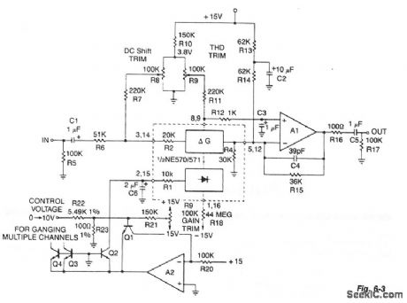
This typical circuit uses an external op amp for better performance and an exponential converter to get a control characteristic of -6 dB/V. Trim networks are shown to null out distortion and dc shift, and to fine trim the gain to 0 dB with 0 V of control voltage. (View)
View full Circuit Diagram | Comments | Reading(0)
Input_protected_differential_input_data__acquisition_system_
Published:2009/7/23 22:10:00 Author:Jessie
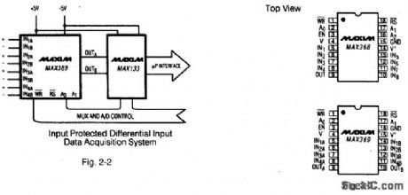
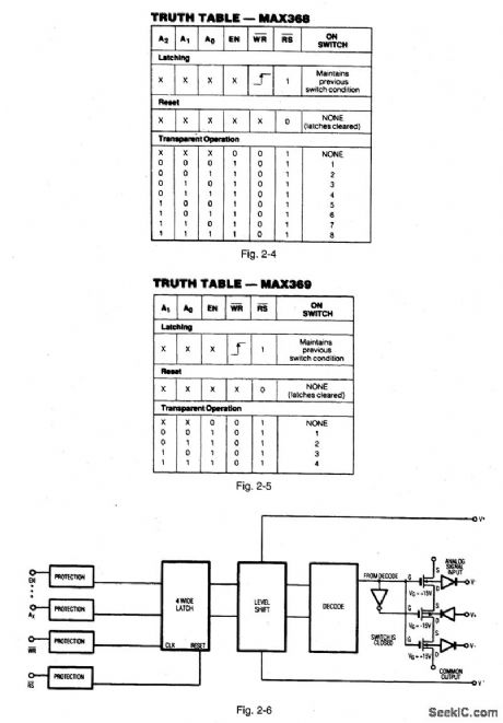


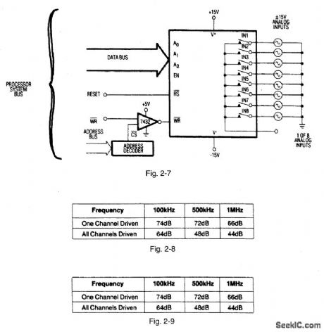
Figures 2-2 and 2-3 show a typical application circuit and pin configurations, respectively, for the MAX368/69,Figures 2-4 and 2-5 show the logic truth tables, respectively, for the MAX368 and MAX369.As shown In Fig,2-6、these fault-protected analog mux ICs have a latch function SO that both write WR and reset RS signals are required. Figure -7 shows the IC connected with a bus interface.Figure 2-8 shows the typical off- isolation rejection ratio. Figure 2-9 shows typical crosstalk-rejection ratio. MAXIM NEW RELEASES DATA Book, 1992,P. 1-31、1-37,1-40,1-44,1-46,1-47. (View)
View full Circuit Diagram | Comments | Reading(664)
SIMPLE_HIGH_VOLTAGE_SUPPLY
Published:2009/7/5 21:37:00 Author:May
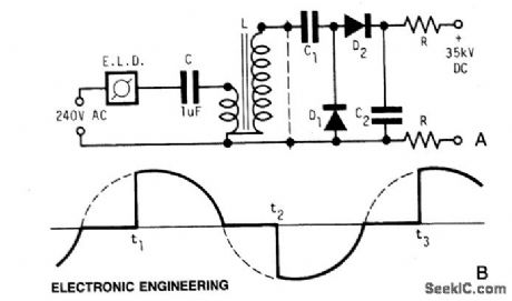
Circuit NotesA light dimmer, a 1 μF capacitor and a 12 V car ignition coil form the simple line powered HV generator. The current in the dimmer is shown in Fig. B. At times t1, t2,..., set by the dimmer switch, the inner triac of the dimmer switches on, and a very high and very fast current pulse charges the capacitor through the primary of the induction coil. Then at a rate of 120 times per second for a 60 Hz line, a very high voltage pulse appears at the secondary of the coil. To obtain an HV dc output, use a voltage doubler. D1 and D2 are selenium rectifiers (TV 18 Siemens or ITT) used for the supply of television sets. High value output shock protection resistors, R, are recommended when suitable. (View)
View full Circuit Diagram | Comments | Reading(0)
Automatic lighting control circuit
Published:2011/7/25 22:37:00 Author:Christina | Keyword: Automatic, lighting control

The core component of the radar type automatic lighting control circuit is the microwave detector module TWH9250. The detection range of this circuit is more than 5m, when someone gets into the detection range, the circuit is triggered, the output port of TWH9250 outputs the low level, the relay K gets power to close, the light turns on, until the person leaves the detection range for 10 seconds, the circuit will reset, the light turns off. The R port of TWH9250 is connected with the photoconductive resistance, so it has minimal resistance value in the day time, the potential of R port is pulled down, the circuit will not work.
(View)
View full Circuit Diagram | Comments | Reading(732)
PROGRAMMABLE_ATTENUATOR
Published:2009/7/5 21:35:00 Author:May
This circuit performs the function of dividing the input signal by a selected constant (1, 2, 4, 8, etc.).While T, Z, or L sections could be used in the input attenuator, this is not necessary since the amplifier loading is negligible and a constant input impedance is maintained. The circuit is thus much simpler and more accurate than the usual method of constructing a constant impedance ladder, and switching sections in and out with analog switches. Two identical circuits can be used to attenuate a balanced line. (View)
View full Circuit Diagram | Comments | Reading(540)
TV_CONTROL_RECEIVER
Published:2009/7/23 22:10:00 Author:Jessie
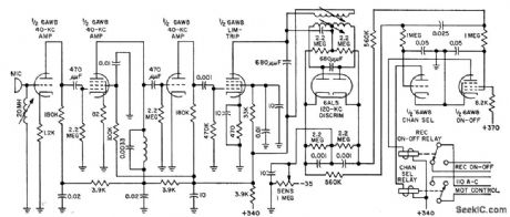
Uses barium titanate transducer as microphone, tuned with 20-mh coil to provide peaks at control frequencies of 38.5 and 41.5 kc. Balanced discriminator detects the two ultrasonic tones. Frequency shift of continuous ultrasonic tone activates tuning-motor relay. Both audio and video are killed during tuning. Also provides remote on. off control of power.-N, Frihart and J. Krakora, Ultrasonic Tones Select Tv Channels, Electronics, 31:23, p 68-69. (View)
View full Circuit Diagram | Comments | Reading(1338)
MEASURING_VALVE_CLOSING_TIME
Published:2009/7/23 22:10:00 Author:Jessie
Determines exact time of valve closure from wave-shape of current in solenoid. Energizing cur rent is differentiated and shaped, to trigger circuits that measure interval between solenoid switch closing and final solenoid osition.-R. L. Kissner, Determining Closure Time in Missile Control Vales, Electronics, 33:42, p 88-89. (View)
View full Circuit Diagram | Comments | Reading(688)
CW_IF_strip
Published:2009/7/23 22:10:00 Author:Jessie
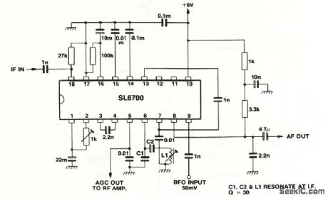
This circuit shows an SL6700 (Fig.2-13)connected to form a CW IF strip with minimum component count,and no ceramlc filter. (View)
View full Circuit Diagram | Comments | Reading(878)
| Pages:1086/2234 At 2010811082108310841085108610871088108910901091109210931094109510961097109810991100Under 20 |
Circuit Categories
power supply circuit
Amplifier Circuit
Basic Circuit
LED and Light Circuit
Sensor Circuit
Signal Processing
Electrical Equipment Circuit
Control Circuit
Remote Control Circuit
A/D-D/A Converter Circuit
Audio Circuit
Measuring and Test Circuit
Communication Circuit
Computer-Related Circuit
555 Circuit
Automotive Circuit
Repairing Circuit