
Circuit Diagram
Index 1080
1_kHz_FAST_START_GATED
Published:2009/7/5 22:30:00 Author:May
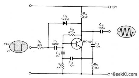
Circuit is conventional phase-shift oscillator in which frequency is determined by C2. C3. C4. R5. R3. and input impedance of transistor. When input is +5 V, almost 100 % negative feedback blocks oscillator. When input drops to0 V. D1 is reversebiased and negative feedback is removed. At same time, edge of input pulse is applied to transistor base to kick off oscillator on its first half-cycle, which is always in phase with falling edge of input signal.-G. F. Butcher. Gated Oscillator with Rapid Start. Wireless World. Aug. 1974. p 272. (View)
View full Circuit Diagram | Comments | Reading(621)
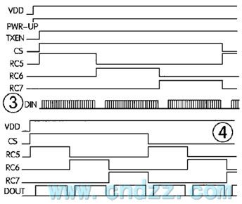
PRECISION_OSCILLATOR_WITH_20_NS_SWITCHING
Published:2009/7/5 22:30:00 Author:May

View full Circuit Diagram | Comments | Reading(631)
FLAME_DETECTOR_DRIVES_TTL_LOAD
Published:2009/7/5 22:29:00 Author:May
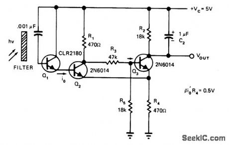
Sensor is silicon Darlington phototransistor Q1 having peak response near infrared bands. Filter is re quired to reduce interference from visible light sources. Circuit is sensitive enough to pick up hydrogen flames that emit no visible light. Article describes operation of circuit and gives design equations. Output can go directly to input port of microprocessor.-A. Ames, This Flame Detector Interfaces Directly to a μP, EDN Magazine, Oct. 20, 1976, p 122 and 124. (View)
View full Circuit Diagram | Comments | Reading(1151)
RECEIVER_FOR_REMOTE_TERMINAL
Published:2009/7/5 22:29:00 Author:May
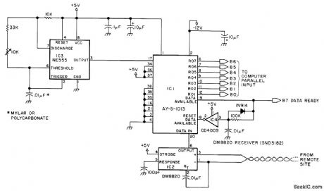
National DM8820 receiver at computer location is connected by twisted-pair line to remote terminal.NE555 oscillator is set at 1760 Hz within 1% with aid of frequency counter, to match corresponding clock in remote terminal. Serial bits coming over line are converted to parallel bits for computer by AY-5-1013 UART. Article gives circuit for remote terminal and covers operation in detail-S. Ciarcia, Come Upstairs and Be Respectable, BYTE, May 1977, p 50-54. (View)
View full Circuit Diagram | Comments | Reading(940)
LINEAR_ANALOG_COUPLER
Published:2009/7/5 22:29:00 Author:May
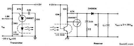
The minimum parts count version of this system provides isolated, linear signal transfer useful at shorter distances or with an optocoupler for linear information transfer.
Although the output is low level and cannot be loaded significantly without harming accuracy, a single LC. operational or instrumentation amplifier can supply both the lin-ear gain and buffering for use with a variety of loads. (View)
View full Circuit Diagram | Comments | Reading(583)
Pincushion correction circuit
Published:2011/7/26 2:59:00 Author:Christina | Keyword: Pincushion correction circuit
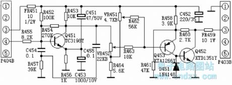
The field sawtooth wave voltage adds to the pincushion correction circuit through the pin-4 of P404, the integral circuit is composed of the R455, C454 and R457, this integral circuit integrates the field sawtooth wave to form the convex parabolic wave voltage, and this voltage adds to the B pole of the parabolic wave plastic amplification tube Q451 to be amplified and reformed, and the C pole outputs the 9V (peak-peak value) concave parabolic wave voltage, this voltage adds to the B pole of the composited tube which is composed of the Q453 and Q452 through the horizontal amplitude adjustment and left & right pincushion distortion adjustment network, so the C pole of the Q452 outputs the 12.5V (peak-peak value) parabolic wave voltage.
(View)
View full Circuit Diagram | Comments | Reading(606)
CLOCK_SOURCE_
Published:2009/7/5 22:29:00 Author:May
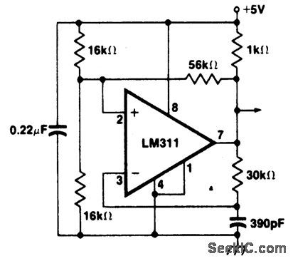
A clock source using LM311 voltage comparator in positive feedback mode to minimize clock frequency shift problem. (View)
View full Circuit Diagram | Comments | Reading(1772)
Sampling Error Amplifier Intergrated Circuit of SE135N
Published:2011/7/29 0:30:00 Author:Michel | Keyword: Sampling Error, Amplifier, Intergrated Circuit

SE135N is a sampling error amplifier intergrated circuit and it is widely used in big screen color TV ,VCD,DVD and kinds of switch power supply.
First,Functions Features
SE135N integrated circuit contains sampling voltage processing circuit, error signal processing circuit, and some other auxiliary function circuit. SE135N IC adopts feet 35 single encapsulation method and its pins functions and data is shown as table 1.
Table 1:SE135N IC Pins Functions and Data (View)
View full Circuit Diagram | Comments | Reading(648)
1_9_kHz_PLL_1
Published:2009/7/5 22:28:00 Author:May

Frequency multiplication is achieved with Signetics NE564 PLL by inserting counter in Ioop between VCO and phase comparator. VCO is then running at multiple of input frequency determined by counter; with connections and values shown, multiplication factor for 60-Hz input signal is 100, giving 6-kHz square-wave output.-''SigneticsAnalog Data Manual,''Signetics, sunnyvale,CA,1977,p 830-831 (View)
View full Circuit Diagram | Comments | Reading(1612)
SCR_GAS_SMOKE_DETECTOR
Published:2009/7/5 22:28:00 Author:May

Simple circuit uses Taguchi TGS308 gas sensor with SCR Q1 for half-wave control of 24-VAC alarm horn.Sensor is based on adsorptive and desorptive reaction of gases on tin oxide semiconductor surface encased in noble-metal heater that serves also as electrode. Combustible gases increase conductivity of sensor, thereby increasing load voltage enough to trip comparator and initiate alarm. Output voltage across Rl is normally about 3 VRMS. With gas or smoke, voltage can rise to 20 V. When gas or smoke has cleared sensor, SCR turns off at first zero crossing. Drawbacks are absence of time delay for preventing false alarm when power istumed on and reduced sound level of horn with half-wave operation.-A. Pshaenich, Solid State Gas/Smoke Detector Systems, Motorola, Phoenix, AZ, 1975, AN-735, p 3. (View)
View full Circuit Diagram | Comments | Reading(1066)
Precious cultural relics radio pursuit device circuit
Published:2011/7/26 3:13:00 Author:Christina | Keyword: Precious, cultural relics, radio pursuit device

The circuit is as shown in the figure. It is composed of the vibration type wireless voice launch circuit, the wireless receiving and demodulation circuit. If you put the transmitter circuit board in the protected cultural relic, when someone moves the historical relic, the press type switch SA will reset, at the same time, the mercury switch SK conducts because of the moving, the VT1 conducts, the sound circuit and the wireless launch circuit get power to send out the voice alarm circuit. When the wireless receiving and demodulation circuit receives the alarm circuit, it will send out the sound of catch the thief! and you can track the thief.
(View)
View full Circuit Diagram | Comments | Reading(886)
FUNCTION_GENERATORI_
Published:2009/7/5 22:27:00 Author:May
View full Circuit Diagram | Comments | Reading(471)
SIMPLE_AC_RELAY_USING_TWO_PHOTON_COUPLERS
Published:2009/7/5 22:27:00 Author:May
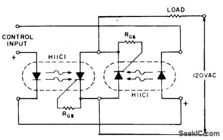
If load current requirements are relatively low (i.e. maximum forward rms current 500 mA), an ac solid state relay can be constructed quite simply by the connection of two H11C optically coupled SCRs in a back-to-back configuration as illustrated. (View)
View full Circuit Diagram | Comments | Reading(547)
LINEAR_AC_ANALOG_COUPLER
Published:2009/7/5 22:27:00 Author:May
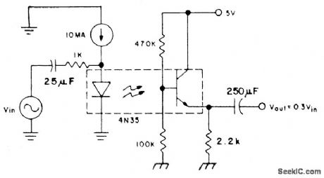
With the coupler biased in the linear region by the 10 mA dc bias on the IRED and the voltage divider on the phototransistor base, photodiode current flows out of the base into the voltage divider, producing an ac voltage proportional to the ac current in the IRED. The transistor is biased as an emitter follower and requires less than 10% of the photodiode current to produce the low impedance ac output across the emitter resistor. Note that the H11AV1 may be substituted for the 4N35 to provide VDE line voltage rated isolation of less than 0.5 pF. (View)
View full Circuit Diagram | Comments | Reading(1983)
Analysing Kewei Home-Use Hand Drier Circuit
Published:2011/7/29 7:32:00 Author:Robert | Keyword: Analysing, Kewei, Home-Use, Hand Drier


The analysis of hand drier circuit's woking principle.The PCB is the main component of the Kewei hand drier. The author has drew this hand drier's full circuit according to the physical PCB, which is shown in picture 1. And the author has also drew this hand drier's working principle diagram by analysing the circuit in picture 1, which is shown in picture 2.1.The power supply circuit.The Kewei hand drier's power supply uses the commercial power 220V as its power supply. The voltage, which the circuit needs, is the DC low voltage (9V). It firstly uses the capacitor C1 to current limiting and voltage step-down. And then it is rectified by diodes D1~D4 and filtered by the electrolytic capacitor C3. At last it would be regulated by the voltage regulator tube Z1. Then it would output the Vcc (9V) DC voltage to supply the hand drier's each part's power. It is added a capacitor C2, C4 for high-frequency pulses filter and a voltage varistor D5 for peak pulse spike limiting in the power loop circuit. (View)
View full Circuit Diagram | Comments | Reading(544)
MCS-51 microcontroller circuit remote controlled by TC9148
Published:2011/7/26 3:32:00 Author:Christina | Keyword: microcontroller circuit, remote controlled
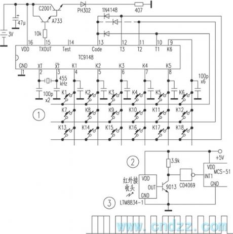
The TC9148 is designed as the CMOS low power consumption infrared remote control launch special IC, and it is usually used with the TC9149/TC9150 infrared remote control receiver IC to control the household appliances.
The principle of the transmitter is as shown in figure 1. The static power consumption of the TC9148 is very low, you need not to set the power switch. The readers also can use the remote controller product that is made with the TC9148. The author codes the first 3 bits of 101 , so the second diode does not need to connect. The principle of the receiver is simple, as the figure 2 shows. The infrared receiver uses the finished product, it sends the signal to the INT1 port of the single-chip microcomputer.
(View)
View full Circuit Diagram | Comments | Reading(2280)
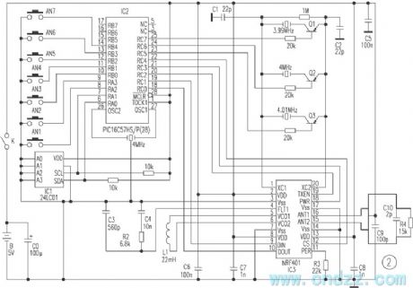
High reliability remote control circuit composed of the monolithic wireless transceiver integrated chip NRF401
Published:2011/7/31 22:17:00 Author:Christina | Keyword: High reliability, remote control, monolithic, wireless transceiver, integrated chip
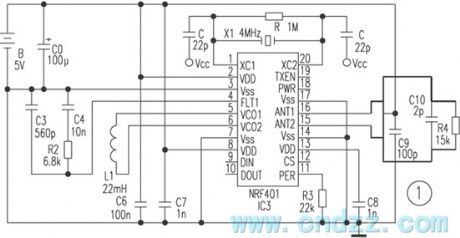
The NRF401 is designed as one kind of digital frequency band 433MHz monolithic wireless transceiver integrated chip which is produced by the Nordic company. This IC has the functions of high-frequency transmitter, high-frequency receiver, PLL synthesizer, FSK modulation, FSK demodulator and multi-channel switch functions.
The circuit is as shown in figure 2. This circuit is the transmitter circuit and the receivier circuit. The SCM IC2 PIC16C57 controls the sending & receiving state and the decoding & coding of the NRF401. When you press the button, the IC2 receives the low level signal, and the pin of IC2 outputs the high level to the pin of IC1 to make the NRF401 get into the launch state. At the same time, this device chooses the different crystals randomly, and it makes the transmitting frequency jump between the six frequency points 432.84MHz, 433.25MHz, 433.92MHz, 434.33MHz, 435.01MHz, 435.42MHz.
(View)
View full Circuit Diagram | Comments | Reading(2123)
Infrared remote control power socket circuit
Published:2011/7/31 22:35:00 Author:Christina | Keyword: Infrared, remote control, power socket

The socket circuit is as shown in figure 1. This circuit uses the receiving, amplification, demodulation integrated infrared receiver, the relay triggers the driving circuit to use one piece of dual D flip-flop MC14013, this circuit uses only one channel of it to connect into the bistable form, the D is connected with the Q, the R and S port are connected with the ground. The R3 and C2 RC networks which are connected with the R port have the power-on reset function, so when the power failure comes again, the socket is in the off state.
In peacetime, the receiving head output port has the 4.2V high level, T2 is in the conduction state, the bistable circuit trigger input port has the low level, the Q port outputs the low level, T1 cuts off, the relay J stops operating, the socket has no 220V output power. If you press the remote controller again, the receiving head will receive the signal of remote controller, and the output port will output the demodulated pulse signal, so the voltage of the output port reduces, the T2 cuts off, the socket losses the power again.
(View)
View full Circuit Diagram | Comments | Reading(2220)
The remote control signal input switching circuit
Published:2011/7/31 22:54:00 Author:Christina | Keyword: remote control, signal, input switching

The digital audio decoder needs a five-choose-one switch to switch three groups of coaxial BS, CD, DAT and two groups of optical signal input. In order to make the digital audio decoder panel concise, we design this kind of switching circuit. This circuit is as shown in the figure.
In this figure, the receiving head receives the remote control pulse signal, and it forms the steep falling pulse edge through the capacitor C to trigger the monostable flip which is composed of the NE555, then the counter CD4017 starts counting, the Q port of it increases one bit, the corresponding relay operats to switch the corresponding input signal. The CD4017 only uses five Q ports, so the pins of it need to connect with each other.
(View)
View full Circuit Diagram | Comments | Reading(914)
The remote control circuit of the toy car
Published:2011/8/1 0:53:00 Author:Christina | Keyword: remote control, toy car

Figure 1 is the remote control circuit, when the control pin of this circuit is connected with the ground, the function which is corresponding to this pin will be in the selective passing state, and it is latched by the latch circuit, the latch signal controls the coding circuit to produce the coded signal that is corresponding to the control function. The carrier signal which is produced by the Q2 and XT is modulated by the coded signal and amplifierd by the Q1. R7 is the oscillation resistance of TX-2, LED is the power supply launch indicator light of the LED.
Figure 2 is the receiving circuit, the high frequency signal which is output by the transmitter is received by the receiving antenna, the super-regenerative receiver circuit is composed of the Q1, L2, C2, C3, the parallel resonant circuit is composed of the L2 and C2, the function of the parallel resonant circuit is frequency selection, C3 is the super-regenerative positive feedback capacitor.
(View)
View full Circuit Diagram | Comments | Reading(4040)
| Pages:1080/2234 At 2010611062106310641065106610671068106910701071107210731074107510761077107810791080Under 20 |
Circuit Categories
power supply circuit
Amplifier Circuit
Basic Circuit
LED and Light Circuit
Sensor Circuit
Signal Processing
Electrical Equipment Circuit
Control Circuit
Remote Control Circuit
A/D-D/A Converter Circuit
Audio Circuit
Measuring and Test Circuit
Communication Circuit
Computer-Related Circuit
555 Circuit
Automotive Circuit
Repairing Circuit