
Circuit Diagram
Index 1075
Low Power Consumption Band-Stop Filter Circuit
Published:2011/7/28 6:29:00 Author:Robert | Keyword: Low, Power Consumption, Band-Stop, Filter
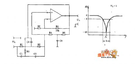
In this circuit the ratio of R6 and R7 would determine the amplification factor Voo in very low frequency. If Vo=1, then the R7 can be cancelled in practice.The selection principle of each elements in this circuit is listed in the picture 2.
500kΩ>R1=R2>1kΩ.0.5uF>C1=C2>200pF.From R1=R2, it has the conclusion that R3=0.5R1. From C1=C2, it has the conclusion that C3=2C1.The quality factor Q=f0/b (-3dB get the point b).It selects R4≈R5=4Q/wC3 and C4=C3/2Q.For example: f0=450Hz, b=250Hz, R1=R2=47kΩ, it has that C1=C2=1/2πf0R=1/2π*450*47*10^3=7.52nF.R3=0.5*4.7kΩ=23.5kΩ.And C3=2C1=15nF.Q=f0/b=450/250=1.8.R4≈R5=4Q/wC3=4*1.8/2π*450*15*10^-9=169kΩ. (View)
View full Circuit Diagram | Comments | Reading(1025)
On_resistance_current_tests
Published:2009/7/23 21:49:00 Author:Jessie

Figure 2-I shows a basic test circuit for measuring on-resistance, r DS(ON) ,for the MAX326/27. Figure 2-J shows how r DS(ON) changes with various analog inputs and supply combinations. Although specified at TTL threshold levels, the logic thresh-old is about 1.5 V± 0.2 V. The IC switches properly with CMOS input levels from -15 V to +15V. Never allow logic levels to exceed supply voltages in any circuit! (View)
View full Circuit Diagram | Comments | Reading(608)
LIGHT_PEN_WITH_INTERFACE
Published:2009/7/5 22:56:00 Author:May
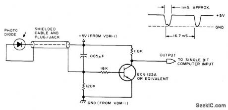
Any high-quality photodiode mounted in discarded housing of marking pen serves as pickup for holding against screen of video display. If diode is mounted in plastic lens, flatten end of lens with emery cloth to give narrower angle of acceptance. Developed for use with VDM-1 display terminal. Use CRO to monitor output as pen is moved across screen. Dark area on screen gives 5-VDC level, and white area gives dips. Article covers use in program design, editing memory dumps, and arranging complex displays.-J.Webster and J. Young, Add a $3 Light Pen to Your Video Display, BYTE, Feb, 1978, p 52, 54 56, and 58. (View)
View full Circuit Diagram | Comments | Reading(885)
Convenient And Simple High-Pass Filter (Differentiator) Circuit
Published:2011/7/30 19:37:00 Author:Robert | Keyword: Convenient, Simple, High-Pass, Filter, Differentiator

The picture shows the convenient and simple high-pass filter (differentiator) circuit.
This circuit is high-pass filter and also could be used as pulse differentiator. The relations between output voltage Ua and input voltage Ue is:Ua=-R1C1(d/dt)Uc.The output voltage's variation value is about 12dB/octave. The frequency point could be determined by the two formulas (picture b).fa=1/2πR1C1=1/2πR2C2, fb=1/2πR2C1.The resistor R3's value is equal with R2's value. (View)
View full Circuit Diagram | Comments | Reading(755)
CASSETTE_BIAS_OSCILLATOR
Published:2009/7/5 22:55:00 Author:May

View full Circuit Diagram | Comments | Reading(674)
Low_cost_instrumentation_amplifier
Published:2009/7/23 21:49:00 Author:Jessie

Compare this simple low-cost circuit to that of Fig 10-15. (View)
View full Circuit Diagram | Comments | Reading(564)
3_V_STROBE
Published:2009/7/5 22:55:00 Author:May
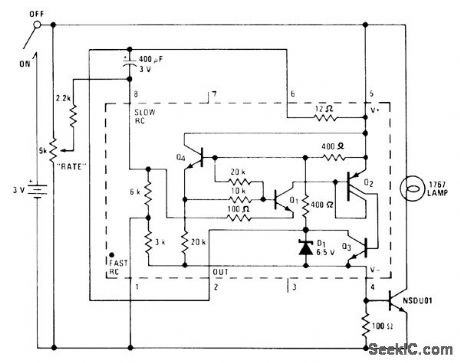
Flash rate of 1767 lamp can be adjusted from no flashes to continuously on, in circuit using National LM3909 flasher IC with extemal NPN power transistor rated at 1 A or higher. Can be used as variable-rate waming Iight, for advertising, or for spedal effects. With lamp in large reflector in dark room, flashes several times per second are almost fast enough to stop motion of dancer.-P. Lefferts, Power-Miser Flasher IC Has Many Novel Applications, EDN Magazine, March 20, 1976, p 59-66. (View)
View full Circuit Diagram | Comments | Reading(546)
RESISTANCE_CONTROLLED_DIGITAL_OSCILLATOR
Published:2009/7/5 22:55:00 Author:May


This very simple, low cost oscillator, is built with two CMOS buffer inverters, two capacitors and a variable resistance. The circuit can work with voltages ranging from 4 V up to 18 V. If C1 = C2, the frequency of oscillation, (ignoring the output and input impedance) is given by:
The graph in Fig. B shows how the output frequency varies with resistance when C1=C2=100 pF and C1=C2=2000 pF.
(View)
View full Circuit Diagram | Comments | Reading(731)
1_Hz_LAMP_BLINKER
Published:2009/7/5 22:53:00 Author:May
Single CMOS flip-flop generates approximately constant low-frequency signal from variable high-frequency signal. RC network in feedback loop determines output frequency, which is independent of rate at which flip-flop is clocked if output frequency is lowerthan dock frequency. If clock frequency is lower, output transitions occur at half of clock frequency. Provides two outputs, approxi-mately equal in duty cycle but opposite in phase. Circuit was developed to blink lamp at 1 Hz to indicate presence of active digital signal having variable duty cycle in range of 100 to 3000 Hz.-V. L. Schuck, Generate a Constant Frequency Cheaply, EDN Magazine, Aug, 20, 1975,p 80 and 82. (View)
View full Circuit Diagram | Comments | Reading(807)
TUNING_CAPACITOR_SIMULATOR
Published:2009/7/5 22:53:00 Author:May
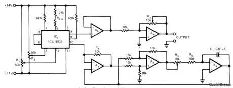
Fixed biasing network is used with Intersil 8038 variable-frequency sine-wave oscillator. Frequency is varied between 175 and 3500 Hz by circuit components forming capacitor simulator. Adjusting R3 varies equivalent capacitor value from 500 pF to 0.01 μF. Distortion is less than 1% overf requency range. Buffer opamp A5 provides high load impedanceto IC1 and low source impedance to variable-gain opamp A6. All opamps are 741.-R, Gunderson, Variable-Fre-quency Oscillator Features Low Distortion, EDN Magazine. Aug. 5. 1974. p 76 and 78. (View)
View full Circuit Diagram | Comments | Reading(765)
Tracking Device Mechanism Diagram Circuit
Published:2011/7/30 9:12:00 Author:Robert | Keyword: Tracking, Device, Mechanism, Diagram
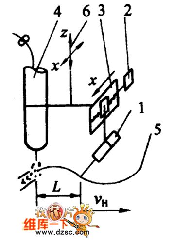
The picture shows the tracking device mechanism diagram circuit.
The part 1 is sensor. The part 2 is stepper machine. The part 3 is screw nut machanism. The part 4 is welding torch. The part 5 is welding with groove. The part 6 is connector (which is connected with the weldment bidirection adjustment mechanism). (View)
View full Circuit Diagram | Comments | Reading(765)
TUNABLE_FREQUENCY_OSCILLATORS
Published:2009/7/5 22:53:00 Author:May


The variable oscillator circuit includes active elements for discharging the timing capacitor CT shown in Fig. 66-7A. A second method is given as in Fig. 66-7B (View)
View full Circuit Diagram | Comments | Reading(731)
SINGLE_CONTROL_FOUR_DECADE_VARIABLE_OSCILLATOR
Published:2009/7/5 22:52:00 Author:May

The circuit consists of a variable current Source that charges a capacitor, which is rapidly discharged by a Schmitt-trigger comparator, The sawtooth waveform thusproduced is fed to another comparator, one with a variable switching level. The outputfrom the second comparator is a pulse train with an independently adjustable frequencyand duty cycle. The variable-frequency ramp generator consists of capacitor C1, which is charged by a variable and nonlinear current source. The latter compnses a 2N2907A pnp transistor, plus resistor R1 and the potentiometer R2 Capacitor C2 eliminates any ripple or nolse at the base ofthe transistor that might cause frequency jitter at the output (View)
View full Circuit Diagram | Comments | Reading(1610)
DRIVING_LED_ARRAY
Published:2009/7/5 22:52:00 Author:May

National MM74C908/MM74C918 dual MOS driver has sections connected as Sdlmitt-trigger oscillator,with R1 and R2 used to generate hysteresis,R3 and C are inverting feedback timing elements, and R4 is pulldown load for first driver. Output current drive capability is greater than 250 mA making circuit suitable for driving array of LEDs or lamps,- CMOS Databook, National Semiconductor,Santa Clara,CA,1977,p 5-38-5-49. (View)
View full Circuit Diagram | Comments | Reading(771)
220_MHz_PHASE_LOCKED
Published:2009/7/5 22:51:00 Author:May
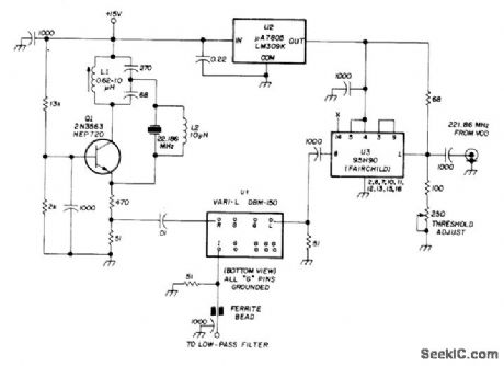
Fairchild 95H90 divide-by-10 counter U3 is used to divide 221.86-MHz VCO output frequency by 10. Resulting 22-MHz output of U3 is compared in phase with output of 22-MHz crystal-controlled oscillator by phase comparator U1, which is standard double-balanced mixer. Output of phase detector is passed through active low-pass filter for control of VCO. Article gives filter and VCO circuits. U2 is 5-V voltage regulator for 95H90.-H.Olson, Frequency Synthesizer for 220 MHz, Ham Radio, Dec. 1974, p 8-14. (View)
View full Circuit Diagram | Comments | Reading(1028)
LOW_VOLTS_ALARM
Published:2009/7/5 22:50:00 Author:May

Circuit Notes
This inexpensive dc supply-voltage monitor sounds a warning when the voltage falls below a preset value. It is ideal for monitoring rechargeable batteries since it draws only a few microamperes when not sounding. The voltage at which the alarm sounds is determined by the zener diode. When the voltage falls below the zener voltage, the alarm sounds. The alarm tone is determined by the RC time constant of the 39 k resistor and 0.01 mf capacitor. (View)
View full Circuit Diagram | Comments | Reading(0)
SHIMMER_FOR_CHRISTMAS_LlGHTS
Published:2009/7/5 22:50:00 Author:May

Circuit uses half of AC cycle to power lights conven-tionally. On other half-cycle, C charges and builds up voltage on gate of SCR When firing point is reached, SCB conducts and allows re mainder of this half-cycle to pass through Iight string. Result is flash that gives shimmer or strobe effect. C is 100-μF 50-V electrolytic, R1 is 2.7K, R2 is 22K, R3 is 3.3K R4 is 100K pot, and R5 is 1K. Diodes are Motorola HEP R0053. SCR is GE C106B1 or Motorola HEP R1221 mounted on heatsink.-R. F. Graf and G. J. Whalen, Add Shimmer to Your Christmas Lights, Popular Science, Dec. 1973, p 1211. (View)
View full Circuit Diagram | Comments | Reading(1396)
VIBRATION_TEST_MONITOR
Published:2009/7/23 22:00:00 Author:Jessie
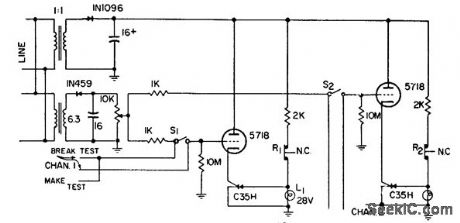
Gives visual indication of momentary contact malfunctions in components during vibration testing. Also indicates permanent open or short. Each channel monitors one component. In testing device having nomally closed contacts, lamp should come on initially. lamp goes out if contacts open momentarily. If lamp remains on offer reset switch for channel is pushed and released, open was momentary. If lamp goes out on release, open is permanent.-Component Vibration Test Monitor, Electronic Circuit Design Handbook, Mactier Pub. Corp., N.Y., 1965, p 159. (View)
View full Circuit Diagram | Comments | Reading(837)
4_MHz_NAND_GATE_OSCILLATOR_SYNCHRO_NIZES_TW0_MPUs_
Published:2009/7/5 22:50:00 Author:May

Low-cost NAND-gate sections A and B form low-cost oscillator for driving two Motorola MC6802 microprocessors.NAND gates C and D function as phase-locked loop, with D ensuring that phases of enable outputs are 180° apart. Small drifts in oscillator frequency do not affect synchronization. Circuit allows each MPU to operate during half-cycle that other MPU has disabled, to provide additional computing power of two microprocessors while maintaining system costs of onedata bus.-J. Farrell, Synchronizing Two Motorola MC6802s on One Bus, Motorola, Phoenix, AZ, 1978, AN-783. (View)
View full Circuit Diagram | Comments | Reading(1302)
Interfacing_D_A_converters_with_HTL_CMOS_and_ECL
Published:2009/7/23 22:00:00 Author:Jessie
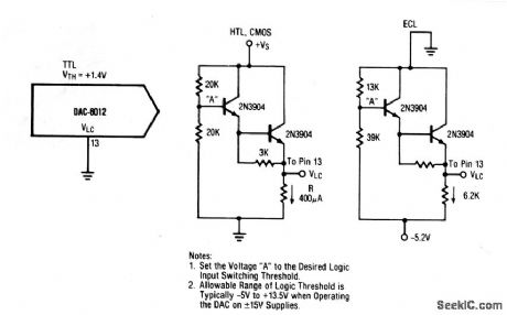
This circuit shows the interface circuits that are required to interface a typical TTL DAC (or similar IC) with ECL, HTL, and CMOS digital devices. Note that PMOS and NMOS devices can generally be interfaced with the CMOS, HTL circuit. (View)
View full Circuit Diagram | Comments | Reading(1734)
| Pages:1075/2234 At 2010611062106310641065106610671068106910701071107210731074107510761077107810791080Under 20 |
Circuit Categories
power supply circuit
Amplifier Circuit
Basic Circuit
LED and Light Circuit
Sensor Circuit
Signal Processing
Electrical Equipment Circuit
Control Circuit
Remote Control Circuit
A/D-D/A Converter Circuit
Audio Circuit
Measuring and Test Circuit
Communication Circuit
Computer-Related Circuit
555 Circuit
Automotive Circuit
Repairing Circuit