
Circuit Diagram
Index 1081
EXPONENTIAL_DIGITALLY_CONTROLLED_OSCILLATOR
Published:2009/7/5 22:27:00 Author:May


The microprocessor-controlled oscillator has a 8159 to 1 frequency range covering 2.5 Hz to 20 kHz. An exponential, current output IC DAC functioning as a programmable current source alternately charges and discharges capacitor between precisely-controlled upper and lower limits. The circuit features instan-taneous frequency change, operates with +5 ±1 V and -15 V ±3 V supplies, and has the dynamic range of a 13-bit DAC. (View)
View full Circuit Diagram | Comments | Reading(763)
General_purpose_RF_amplifier
Published:2009/7/23 22:16:00 Author:Jessie


This circuit is suitable for an SL610C, SL611C, or SC612C. Figure 2-29B-shows the typical voltage gains for the three amplifiers. (View)
View full Circuit Diagram | Comments | Reading(582)
DC_LINEAR_COUPLER
Published:2009/7/5 22:26:00 Author:May
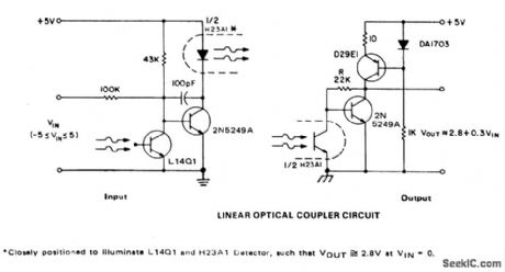
The accuracy of direct linear coupling of analog current signals via an optocoupler is determined by the coupler linearity and its temperature coefficient. Use of an additional cdupler for feedback can provide linearity only if the two couplers are perfectly matched and identically biased. These are not practical constraints in most equipment designs and indicate the need for a different design approach. One of the most successful solutions to this problem can, be illustrated by using a H23 emitter-detector pair and a L14H4, The H23 detector and L14H4 are placed so both are illuminated by the H23 IRED emitter.Ideally, the circuit is mechanically designed such that the H23 emitter may be positioned to provide VOUT=2.8V when VIN=0, thereby insuring collector current matching in the detectors. Then all three devices are locked in position relative to each other.Otherwise, R may be adjusted to provide the proper null level, although temperature tracking should prove worse when R is adjusted. Note that the input bias is dependent on power supply voltage, although the output is relatively independent of supply variations.Testing indicated linearity was better than could be resolved, due to alignment motion caused by using plastic tape to lock positions. The concept of feedback control of IRED power output is useful for both information transmission and sensing circuitry. (View)
View full Circuit Diagram | Comments | Reading(868)
UPPERCASE_DRIVE_FOR_TV_GRAPHICS
Published:2009/7/5 22:25:00 Author:May

Alphameric data-to-video converter using 2513 character generator accepts ASCII words from microprocessor memory and three line commands from instruction decoder. Five dots are outputted simultaneously, corresponding to one row on 5 x 7 dot-matrix character. 7416S eight-input one-output shift register converts dots into serial output video. Input repeats to generate all seven dot rows in row of characters. Shift register is driven by high-frequency timing circuit that delivers LOAD pulse once each microsecond along with CLOCK output running continuously at desired dot rate. Optional cursor uses 4584 5-Hz oscillator for cursor winking rate. If ASCII input bit 8 is high, cursor input goes high and output is white line on leads 01 through 05. Right diode mades this line blink, while Ieft diode allows winking cursors only during valid character times.-D. Lancaster, TVT Hardware Design. Kilobaud, Jan. 1978, p 64-68. (View)
View full Circuit Diagram | Comments | Reading(1562)
Remote control coding transmitting and decoding receiving circuit composed of the M303S/303R
Published:2011/8/1 1:45:00 Author:Christina | Keyword: Remote control, coding, transmitting, decoding, receiving

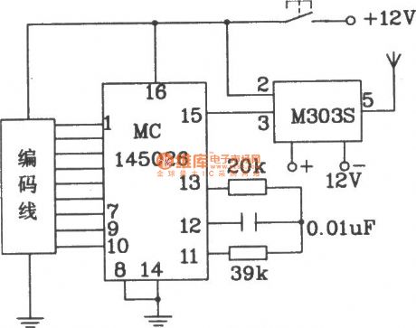


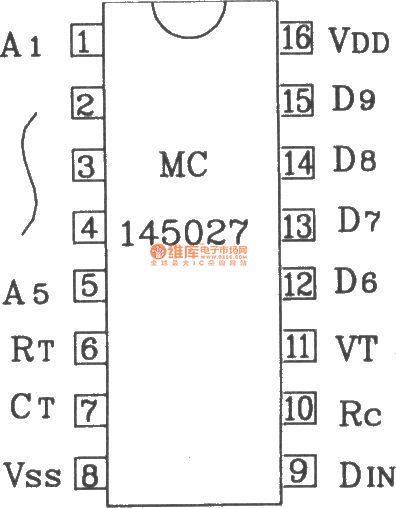
The M303S/303R is designed as one kind of minitype remote control coding transmitting and decoding receiving circuit. It can be used in the short distance data transmission application, because the module uses the dedicated frequency stabilization unit circuit, so the performance of it is stable. This module can be used in the remote control switches, anti-theft alarm devices and the small toys.
The M303S transmitter module is the controllable oscillator & power amplifier unit. The antenna configuration and tuning decides the best operating state of the module, and both of the configuration and tuning directly affect the output power and transmission distance.
(View)
View full Circuit Diagram | Comments | Reading(1183)
One kind of wireless remote control circuit
Published:2011/8/1 1:12:00 Author:Christina | Keyword: wireless, remote control


The remote control transmitter is composed of the DTMF generator and the FM transmitter circuit. Here we use one piece of UM91214B phone specific IC to produce the DTMF signal, the 3V power supply voltage is supplied by the 3V zener tube D1.
The transmitter circuit is composed of the transistor T1 and the external circuits, the tuning circuit L1 and VC1 is tuned at the 100MHz carrier frequency, the antenna uses the whip shape antenna, the length is 10-15cm, the control range is wide. The DTMF signal is sent into the base electrode of T1 through the IC1, and it is output through the antenna ANT.
The receiving part is composed of the DTMF/BCD transform chip IC2 and a group of four trigger latch circuits IC4, IC3. The FM DTMF signal is demodulated by the receiver to change into the BCD signal. At this time the numerical code 1 is the 0001, the numerical code 4 is the 0100.
(View)
View full Circuit Diagram | Comments | Reading(3094)
S1493 Communication Single-chip Microcomputer Integrated Circuit
Published:2011/7/29 8:53:00 Author:Michel | Keyword: Communication Single-chip, Microcomputer, Integrated Circuit


S1493 is a communication single-chip microcomputer integrated circuit, which is widely used in a multi-function call display telephone,such as the 2000 series phones.
First,Functions Features
S1493 integrated circuit is mainly used to complete pulse/double audio dial-up, FSK/DTIMF (frequency shift keying/a frequency system) calling display. Computer controls signal input and output.
Second,Pins Functions and DataS1493 microcomputer integrated circuit uses 80 pins soft packaging way.The liquid crystal display chip packages is directly packaged on printed circuit boards.This structure can greatly improve the reliability of the circuit and also reduce the cost of the circuit.Its pins functions and data are shown as table 1.
Table 1:S1493 IC Pins and Data
(View)
View full Circuit Diagram | Comments | Reading(475)
Audio volume remote control circuit
Published:2011/8/1 1:24:00 Author:Christina | Keyword: Audio volume, remote control

Operating principle: the circuit is as shown in the figure, S is the 4-bit wireless remote control transmitter, Y is the receiving module which is matching with the transmitter. The output ports of Y are amplified by the BG1 ~ BG5 to change the four channels of interlock data control output port signal into the non-latching form, and it controls the electric motor through the relays J1-J4. The M1 controls the main volume, the M2 controls the high and low tones. As the figure 1 shows, the circuit of the electric motors M1 and M2 are the same, also the operating principles. When you press the A button of the transmitter S, the output ports A and I0 of Y output the high level, the BG1 and BG5 conduct. J1 closes, M1 gets power to operate, if you loosen the button, the output of I0 disappears, the electric motor M1 releases to stop working.
(View)
View full Circuit Diagram | Comments | Reading(1352)
IONIZATION_CHAMBER_SENSOR
Published:2009/7/5 22:25:00 Author:May
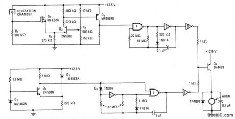
MOSFET Q1 with high input impedance monitors voltage level at divider formed by R1 and ionization chamber, with output of Q1 going to Q2 which forms other half of differential amplifier. With smoke Ievel of 2% orhigher, Q3 is tumed on and applies logic 1 to one input of NAND gate 1 in asymmetrical astable MVBR Capacitor in MVBR charges quickly and discharges slowly, making alarm hom sound during discharge via inverter 3 and driver transistor Q4 Comparator circuit Q5 drives second MVBR to energize hom through inverter 6 and same driver Q4 when battery is low, but with distinctive 1-s toot every 23 s to conserve energy remaining in battery and differentiate from fire waming.-A.Pshaenich and R. Janikowski, Gas and Smoke Detector Uses Low-Leakage MOS Transistor, Electronics, Nov. 28, 1974, p 124-125.
(View)
View full Circuit Diagram | Comments | Reading(1568)
Programmable_gain_amplifier
Published:2009/7/23 22:16:00 Author:Jessie

Figures 2-12 and 2-13 show a typical application circuit and pin configuration/ logic, respectively, for the MAX334, which is a direct replacement for the Siliconix DG271 and HI-201HS. The IC has guaranteed break-before-make switching, tON of 100 ns, tOFF of 50 ns, and channel-on resistance of 50 Ω(max). Split supplies (±5 V to ±15 V) or single positive supplies (+5 V to +30 V) can be used without affecting switching speed or the CMOS/TTL logic-compatible inputs. MAXIM HIGH-RELIABILITY DATA Book, 1993, P. 1-17. (View)
View full Circuit Diagram | Comments | Reading(0)
GATED_OSCILLATOR
Published:2009/7/5 22:24:00 Author:May

View full Circuit Diagram | Comments | Reading(0)
OPERATIONAL_AMPUFIER_SAMPLER
Published:2009/7/23 22:16:00 Author:Jessie

Uses funnel-diode pair with amplifier to provide output that is proportional to input signal at instant corresponding to leading edge of sampling pulse. Voltage gain of circuit is 100.Can also be used to measure differential peak point current of tunnel diode pairs.- Transistor Manual, Seventh Edition, General Electric Co., 1964, p 372. (View)
View full Circuit Diagram | Comments | Reading(603)
Remote control code launching, decoding receiving circuit composed of the F03/J02B
Published:2011/8/1 1:36:00 Author:Christina | Keyword: Remote control code, launching, decoding, receiving circuit
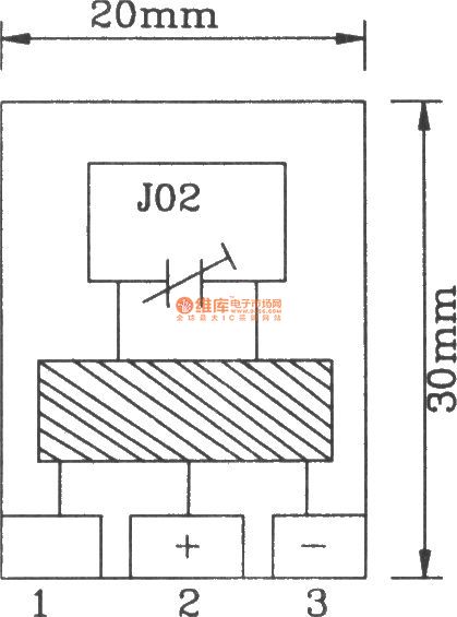
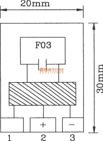
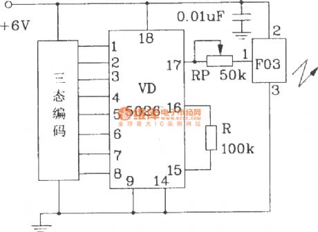

The F03/J02 FM launch/receiving module has the features of small volume, few external components, low voltage power consumption, high efficiency and stable performance. And the module uses the printing plant coil and it operates at the micro-wave side, so the operating frequency is stable and the interference is little, the transmission distance is far, and there is no need to use the external antenna to achieve the effective transmitter / receiver distance. You can use the F03/J02 in the remote control switch, anti-theft alarm, toy and the other electronic equipment control applications. The operating frequency of the F03 transmitter module is about 320MHz.
(View)
View full Circuit Diagram | Comments | Reading(475)
TRANSISTOR_TEST_CIRCUIT
Published:2009/7/23 22:07:00 Author:Jessie
Measures power gain, with emitter current varied manually by R1 in base circuit. Used to determine conditions for uniform emitter current, required for uniform gain in transistor circuits despite variations in d-c beta values of transistors.-K. Redmond, Biasing Transistors for Uniform Gain, Electronics, 33:50, p 74-75. (View)
View full Circuit Diagram | Comments | Reading(647)
MB3813A Charging Circuit
Published:2011/7/23 0:37:00 Author:Michel | Keyword: Charging Circuit
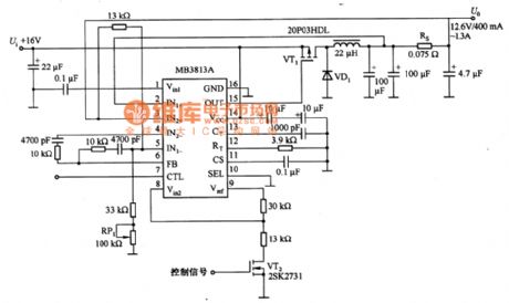
The above pictutre is MB3813A charging circuit.The adjustable output voltage of charging circuit is 12.6 V and output current is 1300 mA or 400 mA.It can charge eight series nimh batteries or 3 quarter series lithium batteries.The maximum current is determined by voltage Ui on V end and current measuring resistance,I。=Ui/25Rs.MB3813A is a constant voltage and current charging controlled integrated controller.Its main feature is that benchmark voltage used by constant current controlling error amplifier can be regulated and the output current can regulate freely. (View)
View full Circuit Diagram | Comments | Reading(416)
REFERENCE_FREQUENCY_SAMPLER
Published:2009/7/23 22:07:00 Author:Jessie
Improves discrimination of f-m signals from magnetic tape, with fastest possible response to wide-deviation frequency-modulated transients. Constant reference frequency is recorded on one tape channel. When playback output voltage is made proportional to quotient of data and reference frequencies, output is independent of tape speed, and wow and flutter components are cancelled. Reference discriminator shown provides voltage output proportional to period of preceding cycle. -P. S. Bengston, Sampling Discriminators for Data Reduction, Electronics, 32:13, p 70-72. (View)
View full Circuit Diagram | Comments | Reading(624)
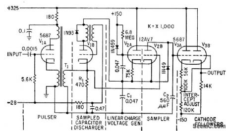
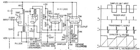
High_power_high_repetition_rate_VSUBPP_SUB_pulse_generator
Published:2009/7/23 22:07:00 Author:Jessie
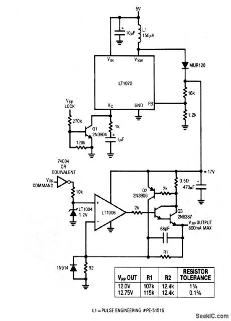
This circuit is similar to the previous VPP circuits, but it has the higher power of the Fig. 6-48 circuit and the higher repetition rate of the Fig. 6-49 circuit. (View)
View full Circuit Diagram | Comments | Reading(493)
DIODE_TESTER_2
Published:2009/7/23 22:07:00 Author:Jessie
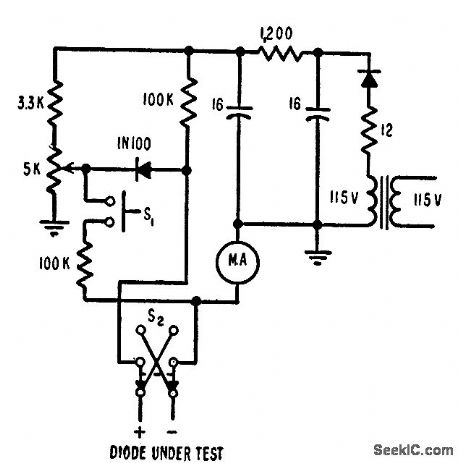
Measures germanium diode reverse (leakage) current rapidly at 50 v back voltage, with no shock hazard and no danger to meter or diode even if diode is shorted or inserted incorrectly. S1 converts meter from ammeter to voltmeter for measuring test terminal voltage. R2 adjusts test voltage to desired half-scale meter reading value. S2 permits checking diode in both directions.-I. J. Levy, Reverse-Current Tester Speeds Diode Checks, Electronics, 31:1, p 88-90. (View)
View full Circuit Diagram | Comments | Reading(815)
MB3759 Charging Circuit
Published:2011/7/23 0:16:00 Author:Michel | Keyword: Charging Circuit

The above pictutre is MB3759 charging circuit.The adjustable output voltage of charging circuit is 12.6 V and output current is 1300 mA or 400 mA.It can charge eight series nimh batteries or 3 quarter series lithium batteries.Its output voltage is set by R1,R2 and RP1.R2 voltage value can be increased by improving output voltage.The output current is controlled by VT3 signal and regulated by R3~R7.And the controlled output current is 1300mA or 400mA.
(View)
View full Circuit Diagram | Comments | Reading(2231)
Low_power_SSB_generator
Published:2009/7/23 22:07:00 Author:Jessie
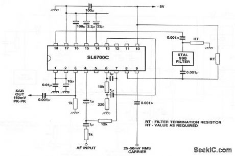
This circuit shows an SL6700 (Fig. 2-13) connected to form a low-power no-adjustment SSB generator. Notice that the microphone input is applied directly to the SL6700. Although this does not provide the same SSB quality as that of the Fig. 2-23 circuit, the savings in components and lower power consumption make the Fig.2-24 circuit attractive for hand-held CB, manpacks,etc. (View)
View full Circuit Diagram | Comments | Reading(1557)
| Pages:1081/2234 At 2010811082108310841085108610871088108910901091109210931094109510961097109810991100Under 20 |
Circuit Categories
power supply circuit
Amplifier Circuit
Basic Circuit
LED and Light Circuit
Sensor Circuit
Signal Processing
Electrical Equipment Circuit
Control Circuit
Remote Control Circuit
A/D-D/A Converter Circuit
Audio Circuit
Measuring and Test Circuit
Communication Circuit
Computer-Related Circuit
555 Circuit
Automotive Circuit
Repairing Circuit