
Circuit Diagram
Index 1097
Serial_controlled_8_channel_SPST_switch_MAX335
Published:2009/7/23 22:22:00 Author:Jessie


Figures 2-22, 2-23 and 2-24 show the functional diagram, pin configuration, and pin description, respect-tively, for the MAX335.Figures 2-25 and 2-26 show the timing, and three-wire interface timing, respectively. Figure 2-27 shows the serial-interface switch programmlng.This IC has eight separately controlled single-pole-single-throw(SPST) switches, all of which conduct equally in either direction, with an on-resistance(100Ω) that is constant over the analog signal range. The switches can continuously operate with supplies from ±4.5 V to ±20 V, and handle rail-to-rail analog signals. Upon power-up, all switches are off, and the internal serial and parallel shift registers are reset to zero. The IC is equivalent to two DG211 quad switches, but controlled by a serial interface. The interface is compatible with both Motorola SPI(Fig.2-28) and Microwire (Fig.2-2),Functioning as a shift register,this serial interface allows data (at DIN) to be clocked In sync with the rising edge of clock (SCLK). The shift register output ( DOUT) enables several MAX335 ICs to be daisy-chained (Fig.2-30), or the ICs can be connected as an addressable serial interface (Fig.2-31) Digital - feedthrough transients are typically 10 mV p-p when a 100-pF capacitance is used at the switch channels.MAXIM NEW RELEASES DATA Book、1995, P. 1-59, 1-64, 1-65, 1-66, 1-67, AND 1-68. (View)
View full Circuit Diagram | Comments | Reading(953)
512_BIT_PROM_PROGRAMMER
Published:2009/7/3 5:20:00 Author:May
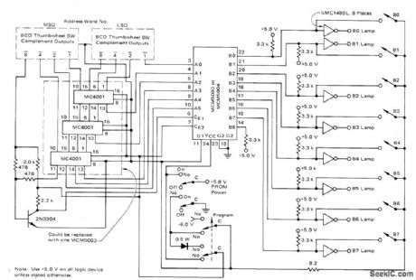
SimpIe manual programmer requires minimum equipment for fusing memory links of Motorola MCM5003 or MCM5004 programmable read-only memory.One link is fused at a time. MC1489 quad line receivers show contents of output bits by driving 5-V 20-mA lamps. Address word number is selected with two BCD thumbwheel switches.Three MC4001 ROMs convert BCD code to that required at address inputs. Program/verify switch must simultaneously be set along withproper output switch for each used bit.-J.E.Prioste, Programming the,MCM5003/5004 Programmable Read Only Memory, Motorola,Phoenix.AZ,1974,AN-550,p4 (View)
View full Circuit Diagram | Comments | Reading(1909)
DC_STBILIZED_FAST_AMPLIFIER
Published:2009/7/3 5:20:00 Author:May
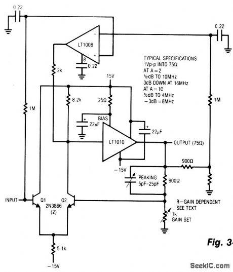
This amplifier functions over a wide range of gains, typically 1 -10. It combines the LT1010 and a fast discrete stage with an LT1008 based dc stabilizing loop. Q1 and Q2 form a differential stage which single-ends into the LT1010. The circuit delivers 1 V pk-pk into a typical 75-Ω video load. At A = 2, the gain is within 0.5 dB to 10 MHz with the -3-dB point occurring at 16 MHz. At A = 10, the gain is flat (± 0.5 dB to 4 MHz) with a -3-dB point at 8 MHz. The peaking adjustment should be optimized under loaded output conditions. This is a simple stage for fast applications where relatively low output swing is required. Its 1 V pk-pk output works nicely for video circuits. A possible problem is the relatively high bias current, typically 10 μA. Additional swing is possible, but more circuitry is needed. (View)
View full Circuit Diagram | Comments | Reading(625)
GAS_SMOKE_SENSOR
Published:2009/7/3 5:19:00 Author:May
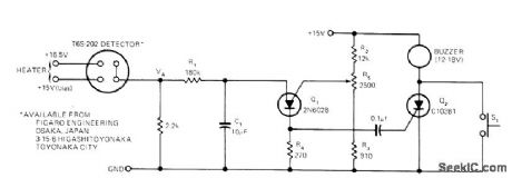
Sensor is based on selective absorption of hydrocarbons by N-type metaloxide surface. Heater in sensor burns off hydrocarbons when gas or smoke disappears, to make sensor reusable. Requires initial warmup time of about 15 min in hydrocarbon-free environment. When gas or smoke is present, VA quickly rises and triggers programmable UJT Q1. Resulting voltage pulse across R4 triggers Q2 and there by energizes buzzer. S1 is reset switch.R1 and C1 give time delay that prevents triggering by small transients such as smoke from cigarette. R5 adjusts alarm threshold. Use regulated supply.-S. J. Bepko, Gas/Smoke Detector Is Sensitive and Inexpensive, EDN Magazine, Sept. 20, 1973, p 83 and 85.
(View)
View full Circuit Diagram | Comments | Reading(1329)
RS_232_transceiver_operated_from__12__and__5_V_power_with_9_V_output
Published:2009/7/23 22:22:00 Author:Jessie

This circuit is useful in PCs where both + 12 V and + 5 are available. The +12 V is connected into one of the charge-pump capacitor pins, rather than the 12V output pin. Supply current decreases to about 9 mA, and -9 V output is available at pin 7. (View)
View full Circuit Diagram | Comments | Reading(578)
TRIAC_GAS_SMOKE_DETECTOR
Published:2009/7/3 5:16:00 Author:May
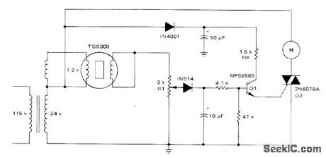
Conductivity of Taguchi TGS308 gas sensor increases in presence of combustible gases, increasing load voltage across R1 from normal 3 VRMS to as much as 20 V. Rise in voltage trips comparator to turn on transistor Q1 that supplies trigger current to 2N6070A sensitivegate triac. Resulting fullwave drive of Delta 1600316824-VAC horn gives sound output of 90 dB at 10 feet. Horn stops automatically when gas clears sensor.-A.Pshaenich, Solid State Gas/Smoke Detector Systems, Motorola, Phoenix, AZ, 1975, AN-735,p4. (View)
View full Circuit Diagram | Comments | Reading(1135)
HEIGHT_SAMPLING_GIVES_NANOSECOND_RESOLUTION
Published:2009/7/23 22:21:00 Author:Jessie
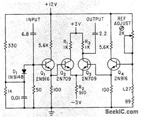
Eight identical four-transistor difference ampli0ers in parallel divide input signal into eight levels for sampling. In each, input signal is compared to reference signal in Q2-Q3.-A. A. Fleischer and E. Johnson, New Digital Conversion Method Provides Nanosecond Resolution, Electronics, 36:18, p 55-57. (View)
View full Circuit Diagram | Comments | Reading(660)
FORWARD_CURRENT_BOOSTER
Published:2009/7/3 5:16:00 Author:May
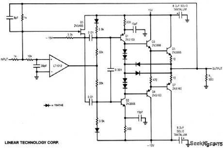
The LT1012 corrects dc errors in the booster stage, and does not set high-frequency signals. Fast signals are fed directly to the stage via Q5 and the 0.01-μF coupling capacitors. Dc and low-frequency signals drive the stage via the op-amp's output. The output stage consists of current sources, Q1 and Q2, driving the Q3 - Q5 and Q4 - Q7 complementary emitter follows. The diode network at the output steers drive away from the transistor bases when output current exceeds 250 mA, providing fast short-circuit protection. The circuit's high frequency summing node is the junction of the 1-K and 10-K resistors at the LT1012. The 10 K/39 pF pair filters high frequencies, permitting accurate dc summation at the LT1012's positive input. This current-boosted amplifier has a slew rate in excess of 1000 V/μS, a full power bandwidth of 7.5 MHz and a 3-dB point of 14 MHz. (View)
View full Circuit Diagram | Comments | Reading(659)
ADDING_FOUR_FU_NCTlONS
Published:2009/7/3 5:12:00 Author:May
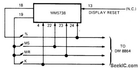
Capability of 8-digit four-function Novus 850 calculator made by National Semiconductor (also marketed as Montgomery Ward P50) can be doubled by adding four SPST swhches and connecting as shown. These provide additional functions of memory store, memory recall, percent, and constant. Switches can be put on front panel above display, at corners of battery. Cutler Hammer SA1BV20 SPST switches with SW53AA1 caps can be squeezed in.-D. Amett, Add Memory, Constant and % to a 4-Function Calculator, EDN Magazine, Aug. 20, 1975, p 82. (View)
View full Circuit Diagram | Comments | Reading(662)
TRANSISTOR_PUMP_DISCRIMINATOR
Published:2009/7/3 5:09:00 Author:May
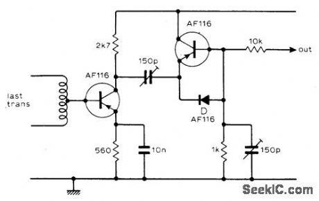
Used with 10.7-MHz IF strip of high-quality FM tuner built from discrete comDonents Circuit is placed between last IF stage and stereo decoder.-W. Anderson, F. M. Discriminator, Wireless World, April 1976, p 63. (View)
View full Circuit Diagram | Comments | Reading(767)
SELF_TUNED_ULTRASONIC_GENERATOR
Published:2009/7/23 22:21:00 Author:Jessie

Current from feedback transducer goes through ballast lamp B1, keeping oscillator circuit V1 tuned to desired frequency between 20 and 40 kc.-S. Vogel, Ultrasonic Equipment in Industry, Electronics, 34:4, p 52-55. (View)
View full Circuit Diagram | Comments | Reading(716)
LEVEL_SHIFTER_FOR_RAM
Published:2009/7/3 5:09:00 Author:May
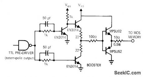
Uses predriverwith three transistors, followed by two-transistor booster, to convert TTL levels to those required by dynamic MOS random-access memory. Booster can be omitted for data input lines be-MEMORY cause they drive such low capacitive loads in typical arrays.-M. E Hoff, Designing an LSI Memory System That Outperforms Cores-Economically,Computer Hardware(section ofEDN Magazine), Jan 15, 1971, p 6-15(p000110-001111) (View)
View full Circuit Diagram | Comments | Reading(586)
AC_COUPLED_DYNAMIC_AMPLIFIER
Published:2009/7/3 5:07:00 Author:May

This circuit acts as a bandpass filter with gain and would be most useful for biomedical instrumen-tation. Low-frequency cutoff is set at 10 Hz while the high-frequency breakpoint is given by the openloop rolloff characteristic of the HA-5141/42/44. In this case, the AVCL= 60 dB where the rolloff occurs at approximately 300 Hz. This comer frequency may be trimmed by inserting a capacitor in parallel with Rf. (View)
View full Circuit Diagram | Comments | Reading(723)
CARRIER_SYSTEM_TRANXMITTER
Published:2009/7/3 5:03:00 Author:May
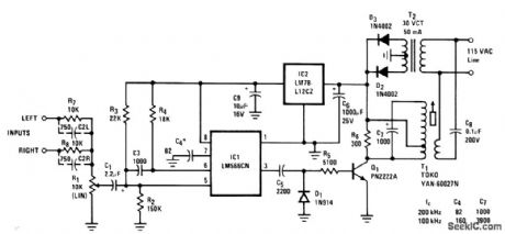
Used to convert audio program material into FM format for coupling to standard power Iines. Modulated FM signal can be detected at any other outlet on same side of distribution transformer, for demodulation and drive of loudspeaker.Input permits combining stereo signals for mono transmission to single remote Ioudspeaker. Uses National LM566CN VCO. Frequency response is 20-20,000 Hz, and total harmonic distortion is under O.5% With 120/240 V power lines, system operates equally well with receiver on either side of line. Transmitter input can be taken from monitor or tape output jack of audio system.-J. Sherwin, N. Sevastopoulos, and T. Regan, FM Remote Speaker System, National Semiconductor, Santa Clara, CA, 1975, AN-146. (View)
View full Circuit Diagram | Comments | Reading(1902)
CARD_CONVERTER
Published:2009/7/3 5:03:00 Author:May

National MM530B ROM forms basis for conversion of 12-line Hollerith punched-card code to 8-line ASCll. All 12 inputs from cards are presented to programmable logic array (PLA). Invalid input produces all-high output state because it is not recognizable product term. First 7 Hollerith lines, which are ordinary decimally coded lines, are encoded to 3 binary lines with additional logic elements shown, before being presented into common 8-input ROM.- Memory Databook, National Semiconductor, Santa Clara, CA, 1977, p 11-49-11-56. (View)
View full Circuit Diagram | Comments | Reading(1343)
Low_drift_integrator
Published:2009/7/23 22:36:00 Author:Jessie
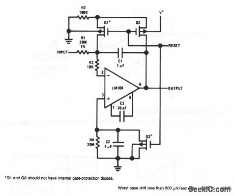
Compare this circuit to that of Fig. 10-41. Hero, the mechanical switch is replaced by Q1 and Q2. (View)
View full Circuit Diagram | Comments | Reading(578)
LOW_PASS_PI_SECTION_AF
Published:2009/7/3 5:00:00 Author:May

Four-pole doublethrow switch gives choice of 650-Hz cutoff for CW or 2000 Hz for SSB.Filter capacitors are matched Response decreases continuously beyond cutoff frequency,with no loss of attenuation.-E.Noll,Circuits and Techniques,Ham Radio,April 1976,p 40-43. (View)
View full Circuit Diagram | Comments | Reading(848)
BROADBAND_HYDROPHONE_PREAMP
Published:2009/7/23 22:36:00 Author:Jessie
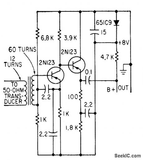
Provides gain of 35 db at 250 kc, with extremely low noise figure (within 1 db of thermal). Operating power of 20 ma d-c can be fed down same RG/8 coax used to transmit signal-R. N. Foss, Transistor Preamp has Very Low Noise, Electronics, 31:29, p 92-96. (View)
View full Circuit Diagram | Comments | Reading(796)
MEMORY_PROTECTING_REGU_LATOR
Published:2009/7/3 5:00:00 Author:May
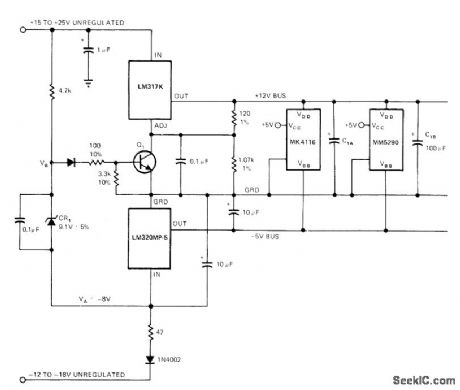
Developed for MOS RAM in which accidental removal of -5 V bias supply would allow buildup of currents flowing between +12 V and ground to value sufficient to open up metal paths and destroy memory. Protection is achieved by feeding unregulated negative voltage to on-card local regulator using LM320MP-5 to provide -5 V regulated bias for all memory chips. LM317K is used as +12 V regulator for delivering up to 1.5 A. If -12 V gradually drops out of regulation, a, turns on and pulls LM317K adjust pin to ground so output of this regulator drops to + 1.3 V and logic circuits are undamaged. If -12 V shorts to ground, capacitors on -5 V line hold up for several hundred microseconds so Q1 has time to turn off +12 V regulator. Use heatsinks for regulators.-R. Pease, Safe Supply Manages MOS Memories, EDNMagazine, Oct. 20, 1978, p 82 and 84. (View)
View full Circuit Diagram | Comments | Reading(654)
80_METER_BANDPASS
Published:2009/7/3 4:59:00 Author:May

Four-resonator filter for use in 80-meter amateur band has 100-kHz bandwidth, 4.4-dB insertion loss, and 6-60 dB shape factor of 5.16. Filter was designed and aligned at 3.75 MHz; realignment at 3.6 and 3.9 MHz yielded Similar results Artiole covers theory.construction, and adjustment-W Hay-ward,Bandpass Filters for Receiver Preselectors,Ham Radio,Feb,1975,p 18-27. (View)
View full Circuit Diagram | Comments | Reading(904)
| Pages:1097/2234 At 2010811082108310841085108610871088108910901091109210931094109510961097109810991100Under 20 |
Circuit Categories
power supply circuit
Amplifier Circuit
Basic Circuit
LED and Light Circuit
Sensor Circuit
Signal Processing
Electrical Equipment Circuit
Control Circuit
Remote Control Circuit
A/D-D/A Converter Circuit
Audio Circuit
Measuring and Test Circuit
Communication Circuit
Computer-Related Circuit
555 Circuit
Automotive Circuit
Repairing Circuit