
Circuit Diagram
Index 1090
OFF_LINE_FLYBACK_REGULATOR
Published:2009/7/5 21:10:00 Author:May
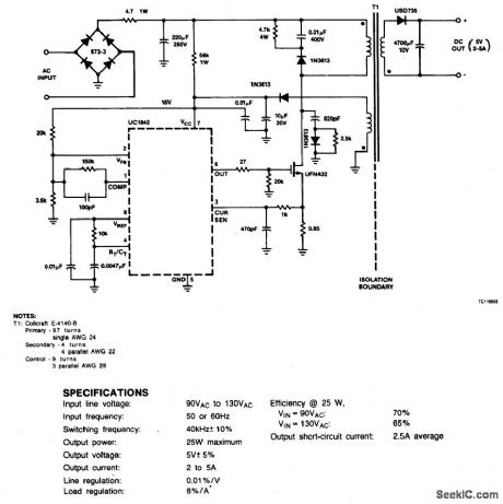
Circuit NotesThis circuit uses a low-cost feedback scheme in which the dc voltage developed from the primary-side control winding is sensed by the UC1842 error amplifier. Load regulation is therefore dependent on the coupling between secondary and control windings, and on transformer leakage inductance. For applications requiring better load regulation, a UC1901 Isolated Feedback Generator can be used to directly sense the output voltage. (View)
View full Circuit Diagram | Comments | Reading(0)
S7230B Microcomputer Dailing Integrated Circuit
Published:2011/7/29 0:40:00 Author:Michel | Keyword: Microcomputer, Dailing, Integrated Circuit

S7230B is microcomputer dailing integrated circuit and it is used in communication device and used as dailing circuit.
S7230B IC adopts feet 22 DIP package and its pins functions and data are shown as table 1.
Table 1:S7230B IC Pins Functions and Data (View)
View full Circuit Diagram | Comments | Reading(668)
ADC
Published:2009/7/5 21:10:00 Author:May

Conversion speed of this design is the sum of the delay through the comparator and the decoding gates. Reference voltages for each bit are developed from a precision resistor ladder network. Values of R and 2R are chosen so that the threshold is 1/2 of the least significant bit. This assures maximum accuracy of ±1/2 bit. The individual strobe line and duality features of the NE521 greatly reduced the cost and complexity of the design. (View)
View full Circuit Diagram | Comments | Reading(2870)
Single_chip_power_supply_with_linear_regulation
Published:2009/7/23 22:59:00 Author:Jessie
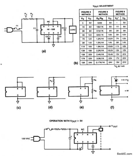
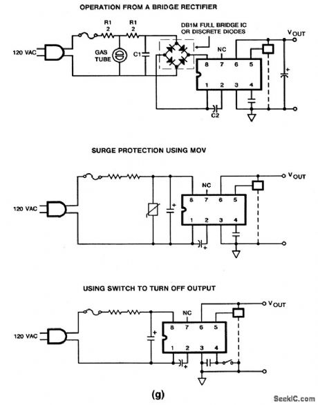
The HV-1205 converts ac into regulated dc to power low-voltage components, such as ICs. Input voltage is 120 V at frequencies from 48 to 380 Hz. Output voltage is set by selection of external components, as shown in the table of Fig. 7-6B, and it can be any value between 5 V and 24V, at 50 mA. Recommended values for components shown in Figs. 7-6C through 7-6G are as follows: fuse F1 is 1/4 A, 2AG; source resistor R1=150 Ω; snubber capacitor C1=0.05μF, ac rated; metal-oxide varistor (MOV, Fig. 7-6G) surge suppressor =V130LA20 or equivalent; pre-regulator capacitor C2 =470μF, with a voltage rating about 10-V greater than chosen VOUT; inhibit capacitor C3=150 pF for 50/60 Hz, and 47 pF for 400 Hz, with a voltage rating about 10-V greater than chosen VOUT; output filter capacitor C4=1μF minimum, 100μF reduced output spikes to about 25 mVp p-p; R2, RA, RB, and VZ=values shown in table Fig. 7-6B (VOUT adjustment). Note that the HV-1205 does not provide isolation from the line. (View)
View full Circuit Diagram | Comments | Reading(945)
STABILIZED_SINE_WAVE
Published:2009/7/5 21:09:00 Author:May

Peak detector is used with FET operated in voltage variable.-resistance mode. in combination with standard double-integration circuit having regenerative feedback. to give 1.46-kHz sinewave output into 500-ohm load at 10 V P-P. Will operate at power supply voltages off 8 to 18 V whhout appreciable variation in output amplitude or frequency. Output varies less than 1.5% in frequency and 6% in amplitude over temperature range of 10 to 65°c. Circuit can be modified for other frequencies.-F. Macli. FET Stabilizes Sine-Wave Oscillator. EDN Magazine. June 5.1973. p 87. (View)
View full Circuit Diagram | Comments | Reading(760)
15_W_AM_amplifier
Published:2009/7/23 22:58:00 Author:Jessie
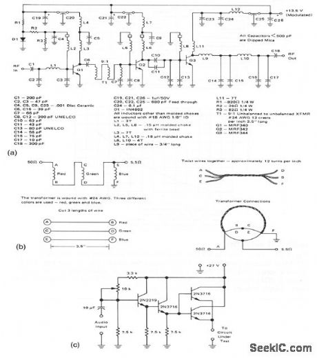
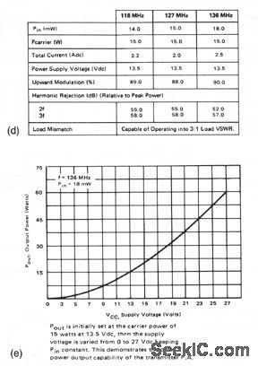
This circuit is a 15-W AM broadband amplifier covering the 118- to 136-MHz aircraft band. Figure 2-52B shows the details for T1, and Fig. 2-52C shows a series modulator that is suitable for testing or modulating the amplifier.Figure 2-52D shows amplifier performance and Fig. 2-52E shows output power versus supply voltage.
(View)
View full Circuit Diagram | Comments | Reading(612)
BX-1393/BX-1408 (TV, video, audio equipment and air conditioner) infrared remote control receiving circuit
Published:2011/8/1 2:55:00 Author:Christina | Keyword: TV, video, audio equipment, air conditioner, infrared, remote control, receiving circuit
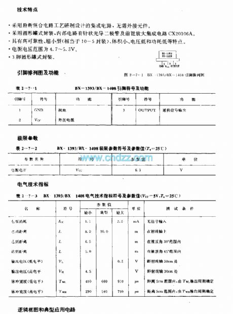

The DX-1393/BX-1408 is designed as one kind of infrared remote control receiving circuit that can be used in the TV, video, audio equipment and air conditioner applications. The carrier frequency of the BX-1393 is 40kHz, the carrier frequency of the BX-1408 is 38kHz.
Features
It uses the latest hybrid circuit technology, so there is no need to use the external components.It uses the circular tank package, the internal circuit has the needle-like optical diode and the preamplifier IC CX20106A.It has the high reliability, ultra-small package, small size, low voltage and low power consumption.The power supply volateg is 4.7-5.3V.The 3-pin circular tank package.
(View)
View full Circuit Diagram | Comments | Reading(3484)
TRACKING_ADC
Published:2009/7/5 21:08:00 Author:May

The analog input is fed into the span resistor of a DAC .he analog input voltage range is selectable in the same way as the output voltage range of the DAC.The net current flow through the ladder termination resistance;i.e.,2 KΩ for HI-562A; produces an error voltage at the DAC output.This error voltage is compared with 1/2 LSB by a comparator. When the error voltage IS within±1/2 LSB range,the Q output ofthe comparators are both low,which Stops the counter and gives a data ready signal to indicate that the digital output is correct,If the error exceeds the±1/2 LSB range,the counter iS enabled and driven In anup or down direction depending on the polarity of the error voltage.
The digital output changes state only when there is a significant change in the analog input.When monitoring a slowly varying input,it is necessary to read the digital output only after a change has taken place.The data ready signal could be used to tngger a flip-flop to indicate the condition and reset it after readout.The main disadvantage of the tracking ADC iS the time required to initially acqutre a signal;for a 12-bit ADC,it could be up to 4096 clock periods.The input signal usually must be filtered so that its rate of change does not exceed the tracking range of the ADC—1 LSB per clock period.
(View)
View full Circuit Diagram | Comments | Reading(1984)
VARIABLE_SLOPE_RAMP_GENERATOR
Published:2009/7/23 22:58:00 Author:Jessie

Slope is determined by rate at which C1 is charged by constant-current generator Q1-R4 through Q2. Peak of ramp is determined by R19. Circuit will synchronize over 3:1 frequency range centered on 70 kc.-D. J. Grover, Capacitor Charging Controls Variable Ramp Generator, Electronics, 39:11, p 91-92. (View)
View full Circuit Diagram | Comments | Reading(1633)
S2569 Microcomputer Dialing Integrated Circuit
Published:2011/7/29 2:54:00 Author:Michel | Keyword: Microcomputer Dialing, Integrated Circuit

S2569 is produced by the British micro system company and it is widely used in communication equipment and dialing circuit.
2569 can produce 12 double audio signal and twelve keyboard correspondent position, which adds repeatation,stitches, pause and flashing functions.The IC has A, B and C series products, the feet 16 DIP package and its pins functions and data are shown as table 1.
Table 1:S2569 IC Pins Functions and Data (View)
View full Circuit Diagram | Comments | Reading(639)
Pulse_generator
Published:2009/7/23 22:57:00 Author:Jessie
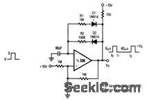
This circuit uses only one section of a 339 comparator and produces pulses of 6-μs duration with 60-μs spacing, using the values shown. Raytheon Linear Integrated Circuts, 1989, p. 5-31. (View)
View full Circuit Diagram | Comments | Reading(0)
PROM_PROGRAMMER_1
Published:2009/7/5 21:05:00 Author:May
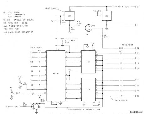
Developed specifically for programming Harris 7641-5 and 7681-5 PROMs, which come with logic 1 in all bit positions. Programmer is used to burn bit at each position requiring logic 0 by process equivalent to blowing fusible link on PROM chip. Process is not reversible, so one emor ruins PROM. Circuit uses two regulator ICs (IC3 and IC4) and two TTL gates (IC1 and IC2). Article gives programming procedure in detail. Software for generating critical timing and control signals with microprocessor is also given.-T. Hayek, Simple and Low-Cost PROM Programmer, Kilobaud, July 1978, p 94-96 and 98-99. (View)
View full Circuit Diagram | Comments | Reading(1914)
Four_phase_stepper_motor_drive_system
Published:2009/7/23 22:57:00 Author:Jessie
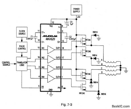
Figure 7-3 shows a MAX620 connected to form a complete stepper-motor drive. TTL/CMOS signals from the logic network are translated to high-side levels that drive four N-channel power MOSFETs, supplying current to each of four stepper-motor phases. The diodes provide a discharge current path for the stepper-motor windings. MAXIM NEW RELEASES DATA BOOk, 1992, P. 4-28. (View)
View full Circuit Diagram | Comments | Reading(1672)
15_Hz_TO_150_kHz_IN_FOUR_RANGES
Published:2009/7/5 21:00:00 Author:May

Switch gives choice of ranges, with R2 and R3 varying frequency in each. Circuit draws only 4mA from two 9-V batteries and provides moderate output at 4-5 V. Connections shown are for TO-5 case of 741.-T. Schultz, Audio Oscillator. QST. Nov. 1974. p 43. (View)
View full Circuit Diagram | Comments | Reading(590)
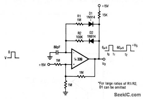
One_shot_multivibrator_with_input_lockout
Published:2009/7/23 22:56:00 Author:Jessie


The input threshold of this comparator IC circuit is set by the resistance from the input to ground. This resistance combines with the series 100-kΩ resistor to form an input lockout. For example, if the input-to-ground resistance is also 100 kΩ, the multivibrator remains off until the input exceeds +8 V. Raytheon Linear Integrated Circuts, 1989, p. 5-30. (View)
View full Circuit Diagram | Comments | Reading(986)
SWITCHED_CAPACITOR_ADC
Published:2009/7/5 20:57:00 Author:May

The CMOS comparator in the successive-approximation system determines each bit by examining the charge on a series of binary-weighted capacitors. In the first phase of the conversion process, the analog input is sampled by closing switch SC and all ST switches, and by simultaneously charging all the capacitors to the input voltage.
In the next phase of the conversion process, all ST and SC switches are opened and the comparator begins identifying bits by identifying the charge on each capacitor relative to the reference voltage. In the switching sequence, all 8 capacitors are examined separately until all 8 bits are identified, and then the charge-convert sequence is repeated. In the first step of the conversion phase, the comparator looks at the first capacitor (binary weight = 128). One pole of the capacitor is switched to the reference voltage, and the equivalent poles of all the other capacitors on the ladder are switched to ground. If the voltage at the summing node is greater than the trip point of the comparator-approximately 1/2 the reference voltage, a bit is placed in the output register, and the 128-weight capacitor is switched to ground. If the voltage at the summing node is less than the trip point of the comparator, this 128-weight capacitor remains connected to the reference input through the remainder of the capacitor-sampling (bit-counting) process. The process is repeated for the 64-weight capacitor, the 32-weight capacitor, and so forth down the line, until all bits are tested. With each step of the capacitor-sampling process, the initial charge is redistributed among the capacitors. The conversion process is successive-approximation, but relies on charge shifting rather than a successive-approximation register-and reference d/a-to count and weigh the bits from MSB to LSB.
(View)
View full Circuit Diagram | Comments | Reading(1263)
PT2275 general infrared remote control decoder circuit
Published:2011/8/1 2:46:00 Author:Christina | Keyword: general, infrared, remote control, decoder
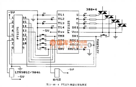

The PT2275 is designed as one kind of general infrared remote control decoder circuit that can be used in the gernal remote control receiving systems. The internal circuit is composed of the oscillator, the timing generator, the code type digital filter, the error checker, the decoder and the output buffer.etc.
Features
Low power consumption.The power supply voltage is 2.2-5.5V.It has eight signal output ports.The start field uses the ordinary code.It has the data inverted signal or non-inverting signal control function and the 1-bit error checking circuit.It has strong anti-interference ability.16-pin dual-row DIP package.The matching model is PT2265.
(View)
View full Circuit Diagram | Comments | Reading(2612)
FET_RAMP_GENERATOR
Published:2009/7/23 22:56:00 Author:Jessie

Use of mos let gives very slow rate-of-rise linear ramp generator (less than 0.1 V/sec). Longer durations can be obtained by using larger values for R and C.-J. M. Phalan, MOS FETs Give Long Time, Constant Ramps, EEE, 14:4, p 46. (View)
View full Circuit Diagram | Comments | Reading(825)
234_kHz_SINE_WAVE
Published:2009/7/5 20:56:00 Author:May

Uses low-cost LM3900N quad differential amplifier IC in lowdistortion oscillator for which third harmonic distortion is typically 0.5%. Peak-to-peak amplitude of sine-wave output is typically 25% of source voltage VCC. Frequency can be changed by altering single component. R3. or by inserting between points B and C an RC network and pot connected as shown in inset. Article gives design equations for frequency and Q.-T. J. Rossiter. Sine Oscillator Uses C.D.A. Wireless World. April 1975. p 176. (View)
View full Circuit Diagram | Comments | Reading(1122)
Dual_linear_regulator_with_high_output_current
Published:2009/7/23 22:56:00 Author:Jessie
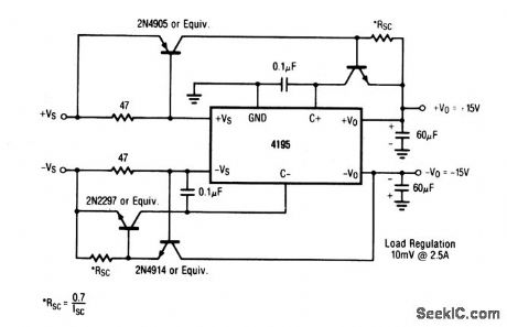
This circuit provides a +15-V and a -15-V output, both of which are capable of delivering 2.5 A. Load regulation is 10 mV at full load. Connection information is shown in Fig. 7-3B. (View)
View full Circuit Diagram | Comments | Reading(672)
| Pages:1090/2234 At 2010811082108310841085108610871088108910901091109210931094109510961097109810991100Under 20 |
Circuit Categories
power supply circuit
Amplifier Circuit
Basic Circuit
LED and Light Circuit
Sensor Circuit
Signal Processing
Electrical Equipment Circuit
Control Circuit
Remote Control Circuit
A/D-D/A Converter Circuit
Audio Circuit
Measuring and Test Circuit
Communication Circuit
Computer-Related Circuit
555 Circuit
Automotive Circuit
Repairing Circuit