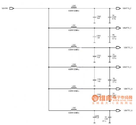
Circuit Diagram
Index 1094
UNDERSEA_PROPAGATION_TRANSMITTER
Published:2009/7/23 22:17:00 Author:Jessie
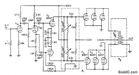
Develops 100-v peak signal across 100-ohm matched resistive load of crystal transducer, for mean power output of 50 w. Is fed by r-f oscillator through transmitter gate that generates voltage pulse whose width is variable from 10 to 5,000 microsec, to turn on transmitter for corresponding time. P1 and P2 are plug-in circuits that must be changed when operating frequency is changed in range of 25 to 150 kc.-W. C. Gore, Ultrasonics Tests Undersea Propagation, Electronics, 31 :35, p 32-35. (View)
View full Circuit Diagram | Comments | Reading(544)
Digital_system_ac_dc_dropout_detector
Published:2009/7/23 22:17:00 Author:Jessie
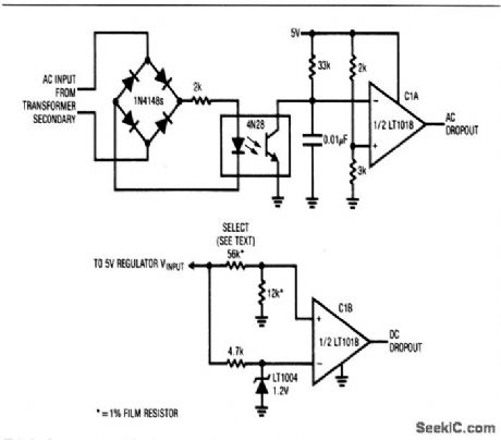
This circuit provides an indication if either or both the ac (line) or dc power to a digital system has dropped out. Fast ac-line dropout detection allows a memory-store command to be issued before dc power fails. Typically, the digital system regulators will continue to supply hold-up power for about 50 to 100 ms after ac-line dropout. This hold-up period (which should be verified in any individual application) permits adequate time to execute a memory-store operation. C1B serves as a final warning that power failure is imminent, by going low when the 5-V regulator drops below the threshold set by the selected resistors. These resistor values should be chosen so that C1B trips when the regulator input approaches the specified dropout voltage. (View)
View full Circuit Diagram | Comments | Reading(2043)
Remote control circuit composed of the TWH9236/9238 miniature radio-controlled component
Published:2011/8/1 2:15:00 Author:Christina | Keyword: Remote control circuit, miniature radio-controlled component

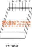
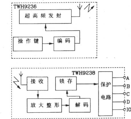

The TWH9236/9238 miniature radio remote control transmitting/receiving component contains a key chain type transmitter and a miniature receiver.
For the launch component TWH9236, the operating voltage is supplied by a Az3 type button cell, the voltage is 1.5V, the operating current is smaller than 6mA. But the operating voltage of the receiving component TWH9238 is 6V, the static current is only 1.5mA. The output voltage of the data output port is 5V, the maximum output current is 1.8mA, so it can drive the transistor directly. The remote control distance is more than 50m.
The TWH9238 can form the 3 and 4-channel remote control transmitting/receiving circuits, also it can be expanded to the 9 and 16-channel remote control circuit.
(View)
View full Circuit Diagram | Comments | Reading(1437)
Simple_SSB_IF_amplifier
Published:2009/7/23 22:17:00 Author:Jessie

This circuit uses three SL612C amplifiers, and provides a gain of 100 dB at 9 MHz. (View)
View full Circuit Diagram | Comments | Reading(496)
Minimizing_phase_distortion_
Published:2009/7/23 22:17:00 Author:Jessie

Figure 2-15 shows a circuit used to minimize phase distortion at a mux output. MAXIM HIGH-RELIABILITY DATA Book, 1993, P. 1-46. (View)
View full Circuit Diagram | Comments | Reading(443)
SAMPLE_AND_HOLD
Published:2009/7/23 22:17:00 Author:Jessie
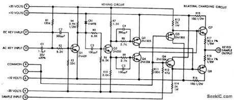
Uses bilateral charging to increase energy content of series of low-duty-cycle amplitude-modulated pulses resulting from demultiplexing one channel of porn pulse train. Designed for sampling and holding 0 to 5 V information received via sampled-data telemetry link.-Sample and Hold Circuit with Bilateral Charging, Electronic Circuit Design Handbook, Mactier Pub. Corp., N.Y., 1965, p 131. (View)
View full Circuit Diagram | Comments | Reading(0)
ZERO_CROSSING_SYNCHRONIZER
Published:2009/7/23 22:16:00 Author:Jessie

Variable-frequency sinusoidal wavetrain output, starting at zero crossing, is produced by gating circuit. Used to determine attenualion and velocity characteristics of ultrasonic delay lines. Covers 20 cps to 300 kc. External blocking oscillator allows use of alternative repetition rate generator when required.-J. A. Wereb, J., Zero-Crossing Technique Syncs Wavetrain Outputs, Electronics, 32:19, p 64-65.
(View)
View full Circuit Diagram | Comments | Reading(0)
Isolating_capacitive_loads
Published:2009/7/23 22:16:00 Author:Jessie

Figure 2-14 shows a circuit used to isolate a mux output that feeds into a large capacitive load. MAXIM HIGH-RELIABILITY DATA Book, 1993, P. 1-46. (View)
View full Circuit Diagram | Comments | Reading(451)
BMW SRS basic circuit diagram
Published:2011/8/1 22:27:00 Author:Ecco | Keyword: BMW SRS , basic circuit
View full Circuit Diagram | Comments | Reading(737)
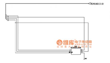
Nokia 6110 circuit diagram 03
Published:2011/8/1 22:13:00 Author:Ecco | Keyword: Nokia 6110
View full Circuit Diagram | Comments | Reading(1194)
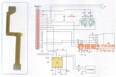
Konka 7388 cell phone cable schematic circuit diagram
Published:2011/8/1 22:31:00 Author:Ecco | Keyword: Konka 7388, cell phone cable
View full Circuit Diagram | Comments | Reading(1054)
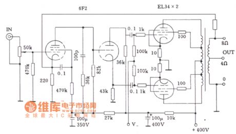
Williams tube amplifier circuit diagram
Published:2011/8/1 22:32:00 Author:Ecco | Keyword: Williams , tube amplifier
View full Circuit Diagram | Comments | Reading(1046)
Dynaco ST70 tube amp circuit diagram
Published:2011/8/1 22:34:00 Author:Ecco | Keyword: Dynaco, tube amp
View full Circuit Diagram | Comments | Reading(2553)
Analog voltage limiter circuit diagram
Published:2011/8/1 22:33:00 Author:Ecco | Keyword: Analog voltage limiter
View full Circuit Diagram | Comments | Reading(700)
300b tube power amp circuit diagram
Published:2011/8/1 22:43:00 Author:Ecco | Keyword: tube power amp
View full Circuit Diagram | Comments | Reading(3919)
Nokia 6110 circuit diagram 04
Published:2011/8/1 22:27:00 Author:Ecco | Keyword: Nokia 6110
View full Circuit Diagram | Comments | Reading(543)
BMW remote control schematic circuit diagram
Published:2011/8/1 22:29:00 Author:Ecco | Keyword: BMW , remote control schematic
View full Circuit Diagram | Comments | Reading(677)
Nokia 6310 circuit diagram 05
Published:2011/8/1 22:28:00 Author:Ecco | Keyword: Nokia 6310
View full Circuit Diagram | Comments | Reading(587)
LOW_FREQUENCY_DOUBLER
Published:2009/7/4 20:59:00 Author:May
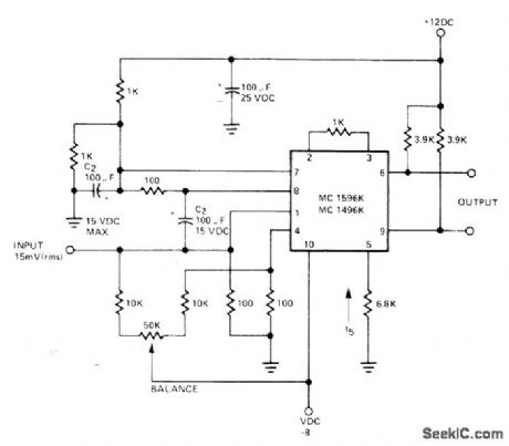
Signetics balanced modulator-demodulator transistor array is connected much like phase detector circuit.Output contains sum component which is twice frequency of input signal because same input signal frequency goes to both sections of balanced modulator.-Signetics Analog Data Manual, Signetics, Sunnyvale, CA, 1977, p 758. (View)
View full Circuit Diagram | Comments | Reading(0)
SIMPLE_DOUBLER_
Published:2009/7/4 20:53:00 Author:May
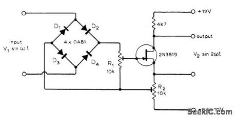
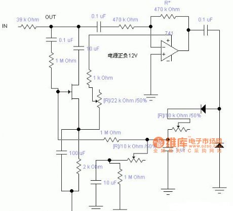
Performance is good up to about 10 kHz. R2 is adjusted to set FET just at cutoff under no-signal conditions, to give operation in square-law region. With R1correctly adjusted, using scope or third harmonic distortion monitor to obtain minimal distoltion, harmonic content of output can be made to approach that of sine-wave input. Article gives design equations.-R. Williams and J. Dunne, Frequency Doubler, Wireless World, Dec. 1975, p 575. (View)
View full Circuit Diagram | Comments | Reading(605)
| Pages:1094/2234 At 2010811082108310841085108610871088108910901091109210931094109510961097109810991100Under 20 |
Circuit Categories
power supply circuit
Amplifier Circuit
Basic Circuit
LED and Light Circuit
Sensor Circuit
Signal Processing
Electrical Equipment Circuit
Control Circuit
Remote Control Circuit
A/D-D/A Converter Circuit
Audio Circuit
Measuring and Test Circuit
Communication Circuit
Computer-Related Circuit
555 Circuit
Automotive Circuit
Repairing Circuit


