
Circuit Diagram
Index 1098
SWITCHABLE_AF_FlLTER
Published:2009/7/3 4:58:00 Author:May

Provides wide range of switch-selected capacitor values for varying cutoff frequencies, to permit use of filter for either phone or CW reception. On CW, circuit improves reception by eliminating higher frequencies that are largely interference.-J. J.Schultz,The Quiet Maker, 73 Magazine, March 1974, p 81-84. (View)
View full Circuit Diagram | Comments | Reading(706)
BASIC_HYBRID_UJT_NPN_TIMER
Published:2009/7/23 22:36:00 Author:Jessie
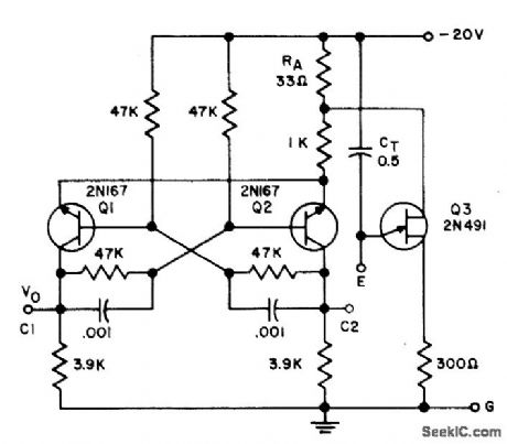
Serves as symmetrical square-wave mvbr when fixed or variable resistor is connected between E and G. Serves as one-shot mvbr when fixed or variable resistor is connected between C1 and E. Other external connections give con stunt or variable-frequency nonsymmetrical multivibrators.- Trcansistor Manual, Seventh Edition, General Electric Co., 1964, p 338. (View)
View full Circuit Diagram | Comments | Reading(629)
AM_BROADCAST_REJECTlON
Published:2009/7/3 4:57:00 Author:May
Seven-element mderived high-pass filter provides 30-dB rejection at AM broadcast-band frequencies while passing signals in 160-meter band. Midsection Inderived branch of circuit was eliminated to simplify construction, but can be added and tuned to particular broadcast station that presents dffficult interference problem. L1 and L3 are 40 turns No. 30 enamel wound on T50-2 powderediron toroid. L2 has 22 turns No. 30 on T50-2 core.-D. DeMaw, Low-Noise Receiving Antennas, QST, Dec. 1977, p 36-39. (View)
View full Circuit Diagram | Comments | Reading(618)
ENCODER_COMMUTATOR
Published:2009/7/23 22:35:00 Author:Jessie
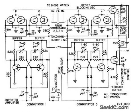
Commutator, buffer, und feedback circuits are given for elapsed-time encoder. After oscillator has triggered 24 elapsed-time counters during storage period, oscillator is switched to electronic commutator controlling diode matrix switch. Counter data is then read out serially through matrix and fed to crt for photo-graphing.-R. J. Kelso and J. C. Groce, Encoder Measures Random Event Time Intervals, Electronics, 32:12, p 48-51. (View)
View full Circuit Diagram | Comments | Reading(621)
693_2079_Hz_TUNABLE_NOTCH
Published:2009/7/3 4:56:00 Author:May

Requires only one tuning pot to cover entire frequency range.Developed for use in tunable narrow-band audio amplifier. Article gives design equations.Depth of notch is greater than 50 dB. Doubling capacitor values changes tuning range to 355-1028 Hz, while cutting values in half gives range of 1340-4110 Hz.-C. Hall, Tunable RC Notch Filter, Ham Radio, Sept. 1975, p 16-20. (View)
View full Circuit Diagram | Comments | Reading(639)
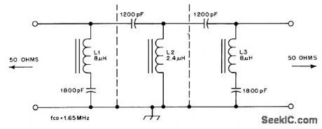
225_Hz_BANDPASS_RTTY
Published:2009/7/3 4:55:00 Author:May

Used ahead of Limiter in 170-Hz-shift RTTY receiving converter.Chebyshev mesh configuration with 0.1-dB ripple uses inductor to ground for sharpening lower skirt, with capacitive coupling for sharpening upper skirt, to give good symmetry for response curve. Capacitors should be high-Q ty low in frequency. Insertion loss is 6.6 dB and 3-dB bandwidth is 225 Hz, which makes mark and space tones only 1.5 dB down.-A. J. Klappenberger, A High-Performance RTTY Band-Pass Filter, QST, Jan. 1978, p 33. (View)
View full Circuit Diagram | Comments | Reading(590)
Tuned_amplifier_MP_pinout
Published:2009/7/23 22:35:00 Author:Jessie
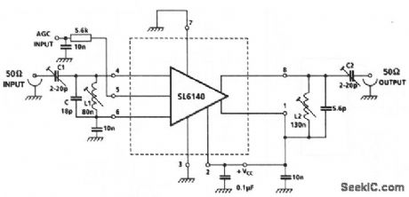
This circuit shows an SL6140 wideband AGC amplifier used as a 100-MHz tuned amplifier with a power gain of 35 dB (Fig 2-19). The high gain is achieved at the expense of bandwidth by means of the matching networks. L1 and L2 are adjusted to set the tuned frequency. C1 and C2 are adjusted to optimize gain.However, if too high an impedance is seen by the input or output, the circuit might oscillate. Adjust C1 and C2 for the minimum bandwidth necessary for the particular application. For best results, use a 50-Ω track ground plane from the matching networks to the 50-Ω source and load. (View)
View full Circuit Diagram | Comments | Reading(691)
FM_DETECTOR_
Published:2009/7/3 4:50:00 Author:May

SingLe IC can be added to any receiver not having FM detector. Moving C2 from pin 9 to pin 10 gives higher audio output.Receivers having Less than 5 kHz IF bandwidth can be broadened by stagger-tuning IF strip slightly to improve audio clarity. Adjust tuned circuit of detector for maximum recovered audio.-I. Math, Math's Notes, CQ, June 1972, p 49-51 and 80. (View)
View full Circuit Diagram | Comments | Reading(873)
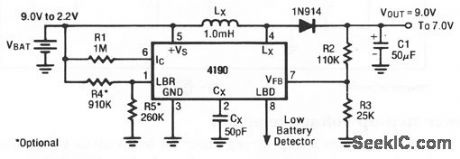
Buck_boost_voltage_regulator
Published:2009/7/23 22:35:00 Author:Jessie
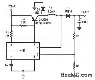
A disadvantage of the standard step-up and stop-down circuits is the limitation of the input voltage range. For a step-up circuit (Fig. 4-2), the battery voltage must always be less than the programmed output voltage, and for a step-down circuit (Fig. 4-3), the battery voltage must always be greater than the output voltage. Figure 4-8 eliminates this disadvantage, and allows a battery voltage above the programmed output voltage to decay to well below the output voltage. The values of R2 and R3 are determined, as described for Fig. 4-2. (View)
View full Circuit Diagram | Comments | Reading(740)
MULTI_WAVEFORM_GENERATOR
Published:2009/7/23 22:35:00 Author:Jessie

Uses double-bootstrap sweeps to generate triangular wave. Can be free-running or driven by external generator. Polarity-sensitive trigger circuit controls sweeps.-J. E. Curry, Multi-Waveform Generator, Electronics, 32:46, p 83. (View)
View full Circuit Diagram | Comments | Reading(662)
05MHz_WITH_20_DEVIATION_
Published:2009/7/3 4:45:00 Author:May
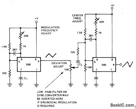
One 566 function generator serves for generating relatively low-frequency carrier (center frequency less than 0.5 MHz), and other 566 serves as modulator producing triangle output with frequency determined by C1. Combination is suitable for deviations up to ±20% of carrier frequency.- Signetics Analog Data Manual, Signetics, Sunnyvale, CA, 1977, p 852-853. I (View)
View full Circuit Diagram | Comments | Reading(574)
RESPONDER_FOR_13_KC_DOG_WHISILE
Published:2009/7/23 22:35:00 Author:Jessie
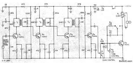
Tuned stages Q1-Q2-Q3 each having 700cps bandwidth, staggered to give total bandwidth of 1.7 kc for amplifier. Untuned stage Q4 maximizes gain yet prevents operation of device by circuit noise. Diode detector D1 makes Q5 conduct, energizing relay K1 and sounding response bell for 25 sec(controlled by charging of C3).-M. R. McGraw and I. Aleksander, Ultrasonic Frequency Responder Aids Blind, Electronics, 34:43, p 48-49. (View)
View full Circuit Diagram | Comments | Reading(541)
650_MHz_AMPLIFYING_PRESCALER_PROBE
Published:2009/7/3 4:44:00 Author:May
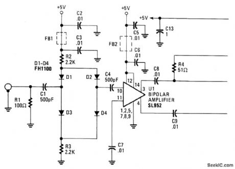
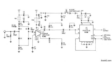
CircU1t Notes
The 650 MHz Prescaler Probe's input is terminated by resistor R1 and is fed through C1 to the diode limiter composed of D1 through D4. Those diodes are forward-biased by the + 5 volt supply for small-input signals and, in turn, feed the signal to U1. Howev-er, for larger input signals, diodes Dl through D4 will start to turn off, passing less of the signal, and, thus, attenuating it. But even in a full-off state, the FH1100-type diodes will always pass a small part of the input to U1 because of capacitive leakage within the diodes. Integrated circU1t U1, a Plessey SL952 bipolar amplifier, capable of 1 GHz operation, provides 20 to 30 dB of gain. The input signal is supplied to pin 10, U1 withthe other input (pin 11) is bypassed to ground. The output signal is taken at pin 3 and pin 4, with pin 3 loaded by R4 and pin 4 by R5.Integrated circU1t 11C90, U2, is a high-speed prescaler capable of 650 MHz operation configured for a divide-by-10 format. A reference voltage internally generated appears at pin 15 and is tied to pin 16, the clock input. This centers the capacitive-coupled input voltage from U1 around the switching threshold-voltage level. An ECL-to-TTL converter in U1 provides level conversion to drive TTL input counters by typing pin 13 low.Therefore, no external EOL to TTL converter is reqU1red at the pin 11 output. On the other hand, EOL outputs are available at U2, pin 8 (Q4) and at pin 9 (Q4), if desired.In that circU1t configuration, pin 13 is left open, and U2 will use less power. (View)
View full Circuit Diagram | Comments | Reading(3234)
PROM_BURNER
Published:2009/7/3 4:44:00 Author:May

Meets radically different pro grahiming requirements for 8223 and 82S23 ROMs. S1 and S2 ale BCD thumbwheelswitches that select word address in octal. S3 select output bit to be programmed or verified.S4 is pushed momentarily to burn out programmed bit, and S5 verifies programming. S6 is set to PROM type, and S7 puts 12-V zeneracross 19-V zener for current calibration. For 82S23, adjust power suppliesto 10 and 21 V and adjust 25-ohm pot to give meter reading of 65mA when S7 is closed.-VV,J Hosking.Finally!A Simple PROM Burner! 73 Magazine, Dec.1977,p 186-187 (View)
View full Circuit Diagram | Comments | Reading(1832)
Electric and pressure measuring circuit diagram
Published:2011/8/1 21:01:00 Author:Ecco | Keyword: Electric measuring , pressure measuring

Figure (a) shows the general test pencil circuit; figure (b) shows the sound test circuit; Figure (c) shows the pressure measurement circuit with flashing light; figure (d) is the voltage indication circuit; figure (e) shows the peak voltage indicator circuit, and adjusting the resistance of the potentiometer RP can increase gradually neon starter.
(View)
View full Circuit Diagram | Comments | Reading(873)
Instrumentation_amplifier_with_±_100_V_common_mode_range
Published:2009/7/23 22:34:00 Author:Jessie
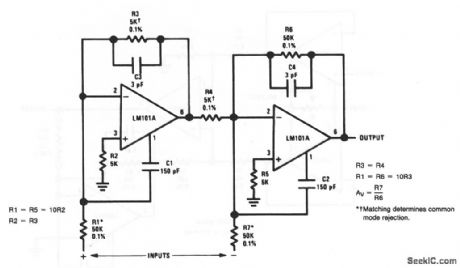
This circuit provides a much higher common-mode range than that of Fig.10-49,but has a lower input impedance. (View)
View full Circuit Diagram | Comments | Reading(729)
RECYCLING_WITH_VARIABLE_DUTY_CYCLE
Published:2009/7/23 22:34:00 Author:Jessie

Two 100K variable resistors control on and off times. Gives time delays from 0.3 to 6 sec.-P. Gheorghiu, Recycling Timing with Variable Duty-Cycle, EEE, 13:4, p 41. (View)
View full Circuit Diagram | Comments | Reading(737)
Bootstrap_voltage_regulator
Published:2009/7/23 22:34:00 Author:Jessie
In this circuit, power to the IC is taken from the output voltage by connecting the +Vs pin and the top of R1 to the output voltage. Notice that the initial battery voltage must be greater than 3.0 V when the circuit is energized. If not, there will not be enough voltage at pin 5 to start the IC. The big advantage of this circuit is the ability to operate down to a discharged battery voltage of 1.0 V.The value of C1 is determined, as described for Fig. 4-2. (View)
View full Circuit Diagram | Comments | Reading(778)
Serially_programmable_VHF_frequency_synthesizer_1
Published:2009/7/23 22:34:00 Author:Jessie
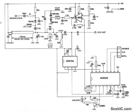
This circuit uses an NJ8822 single-chip synthesizer, an SP8793 dual-modulus prescaler, and an SL562 low-noise op amp to form a frequency synthesizer, with an output range from 144 to 146 MHz at a level of +3 dBm into 50Ω. The lock-up time for a 1-MHz change in frequency is 80 ms. The NJ8822 is programmed via a serial microprocessor interface. The VCO (using a coax resonator) is modulated by applying audio to the cathode of a reverse-biased PIN diode. The loop filter uses the SL562, which has a loop bandwidth of 60 Hz (with the values shown) and a damping factor of 0.6. The filter is followed by a low-pass pole at 3.7 kHz to attenuate the 12.5-kHz reference sidebands. (View)
View full Circuit Diagram | Comments | Reading(1223)
Double-barreled single-block circuit diagram
Published:2011/8/1 21:21:00 Author:Ecco | Keyword: Double-barreled , single-block
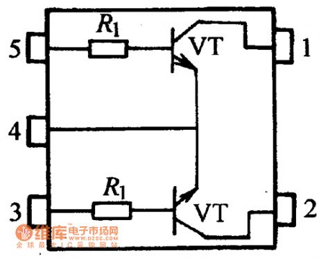
The main transistor with resistance is a kind of small power tube, which is used as the electronic switch or inverter in household appliances and other electronic devices. Some band-stop tubes contain two transistors and lead 5-6 feet (dual-barreled single-resistance model, it is shown in Figure)
(View)
View full Circuit Diagram | Comments | Reading(478)
| Pages:1098/2234 At 2010811082108310841085108610871088108910901091109210931094109510961097109810991100Under 20 |
Circuit Categories
power supply circuit
Amplifier Circuit
Basic Circuit
LED and Light Circuit
Sensor Circuit
Signal Processing
Electrical Equipment Circuit
Control Circuit
Remote Control Circuit
A/D-D/A Converter Circuit
Audio Circuit
Measuring and Test Circuit
Communication Circuit
Computer-Related Circuit
555 Circuit
Automotive Circuit
Repairing Circuit