
Circuit Diagram
Index 1096
ZERO_ORDER_DATA_HOLD
Published:2009/7/23 22:19:00 Author:Jessie
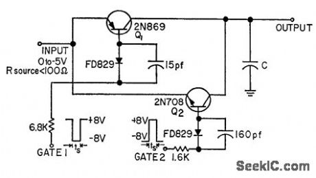
Samples analog signal and holds sample value for period much longer than sampling aperture, as required in some sampled data systems and analog-to-digital converters. Used to sample inputs to accuracy of 0.1% of full scale, using sampling aperture greater thorn 1.25 microsec. Value of C is equal to sampling aperture divided by resistance in charge and discharge path.-E. Nelson, Zero. Order Data Hold, FEE, 11:7, p 26-27. (View)
View full Circuit Diagram | Comments | Reading(810)
REMOTE_TV_VOLUME_CONTROL
Published:2009/7/23 22:19:00 Author:Jessie

Ultrasonic bursts from handheld transmitter are picked up by microphone and fed to ujt threshold detector 2N2646 that also generates trigger pulse. Two cascaded bistable dividers control three transistors shunted across volume control, to give full volume (no shunting) and three lower volume levels.-J. H. Phelps, Transistors Instead of Relays Tune TV Volume, Electronics, 37:9, p 32-33. (View)
View full Circuit Diagram | Comments | Reading(659)
CRYSTAL_DISCRIMINATOR_
Published:2009/7/4 4:00:00 Author:May

Inexpen sive third-overtone CB crystal used at 9-MHz fundamental serves as high-performance discriminator for VHF FM receiver. Adjust C3 for zero voltage with unmodulated carrier at or near center frequency. Adjust CI and C2 with AF sine wave applied to FM signal generator, using CR0 to check distortion of recovered sinewave. With 1 V P-P IF signal at 9 MHz and 5-kHz deviation, recovered audio will be about 1 V P-P at lower audio frequencies. Good limiter is required ahead of discriminator for AM rejection.-G. K.Shubert, Crystal Discriminator for VHF FM, Ham Radio, Oct. 1975, p 67-69. (View)
View full Circuit Diagram | Comments | Reading(2313)
IMPROVED_THYPATRON_TIMER
Published:2009/7/23 22:19:00 Author:Jessie
Linearity is improved by varying capacitance rather than resistance in grid circuits. riming error is less than 1% for 1 to 400 sec.-R. L. Ives, Timer Made More Linear, Electronics, 32:5, p 66-69. (View)
View full Circuit Diagram | Comments | Reading(531)
TONE_PROBE_FOR_TESTING_DIGITAL_ICs
Published:2009/7/3 5:28:00 Author:May
Circuit Notes
The tone probe uses sound to tell the status of the signal being probed. The probe's input circuit senses the condition of the signal and produces either a low-pitched tone for low-level signals (less than 0.8 V) or a high-pitched tone for high-level signals (greater than 2 V). (View)
View full Circuit Diagram | Comments | Reading(1756)
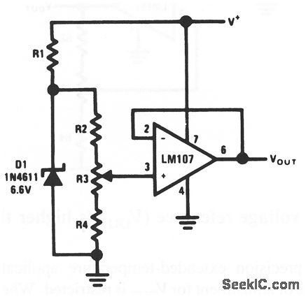
Positive_variable_voltage_reference_vout_is_higher_than_reference_zener
Published:2009/7/23 22:19:00 Author:Jessie
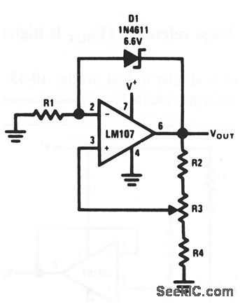
High-preclsion extended-temperature applications of this circult require that the range of adjustment for VOUT is restricted,When this is done,R1 can be chosen to provide optimum zener current for minimum zener temrerature coefficient (TC). Because zener current IZ is not a function of V+,reference TC is independent of V+.
(View)
View full Circuit Diagram | Comments | Reading(572)
CLOCK_DRIVER
Published:2009/7/3 5:25:00 Author:May
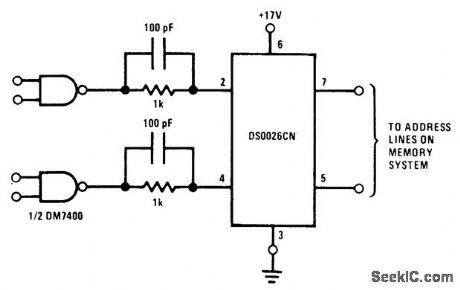
Circuit uses National DS0026CN monolithic clock driver as directcoupled driverfor address or precharge lines on MM1103 RAM at frequencies above 1 MHz. Can be driven by standard TTL gates and flipflops.- Memory Databook, National Semiconductor, Santa Clara, CA, 1977, p 11-27-11-36. (View)
View full Circuit Diagram | Comments | Reading(650)
VOLTAGE_FOLLOWER_AMPLIFIER_FOR_SIGNAL_SUPPLY_OPERATION
Published:2009/7/3 5:25:00 Author:May
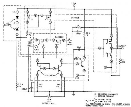
This unity-gain follower amplifier has a CMOS p-channel input, an npn second-gain stage, and a CMOS inverter output. The IC building blocks are two CA3600E's (CMOS transistor pairs) and a CA3046 npn transistor array. A zener-regulated leg provides bias for a 400-μA p-channel source, feeding the input stage, which is terminated in an npn current mirror. The amplifier voltage-offset is nulled with the 10-KΩ balance potentiometer. The second-stage current level is established by the 20-KΩ load, and is selected to approximately the first-stage current level, to assure similar positive and negative slew rates. The CMOS inverter portion forms the final output stage and is terminated in a 2-KΩ load, a typical value used with monolithic op amps. Voltage gain is affected by the choice of load resistance value. The output stage of this amplifier is easily driven to within 1 mV of the negative supply voltage. (View)
View full Circuit Diagram | Comments | Reading(1324)
Memory_save_at_power_down
Published:2009/7/23 22:19:00 Author:Jessie
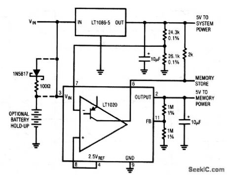
This dc-sensing circuit is useful where ac-line dropout (Fig. 6-54) is not feasible. The circuit uses the different dropout voltages of two regulators. When VIN input power (which could be from a battery or filter capacitor) falls, the LT1086 drops out first. This is detected by the LT1020 comparator, which goes low to alert the memory section (MEMORY STORE). The LT1020 regulator output maintains memory power for additional time, but finally begins to fall about 50 ms after the MEMORY STORE command. The optional connections shown allow extended hold-up times. (View)
View full Circuit Diagram | Comments | Reading(583)
PROM_PROGRAMMER
Published:2009/7/3 5:23:00 Author:May
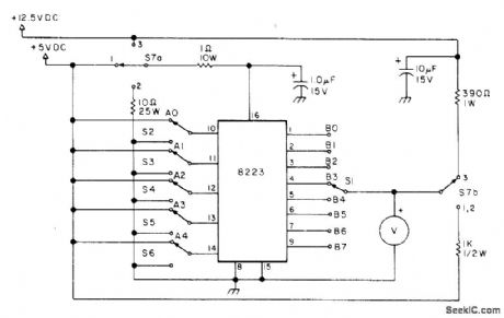
Can be used to blow links one by one, as required, on 8223 programmable read-only memory and on 82S23 Schottky version. Article covers construction, pretesting, and operation.-R. M. Stevenson, An 82S23 PROM Programmer!, 73 Magazine, June 1977, p 82-83. (View)
View full Circuit Diagram | Comments | Reading(2149)
LOW_NOISE_PHOTODIODE_AMPLIFIER
Published:2009/7/3 5:23:00 Author:May
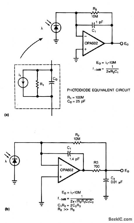
Adding two passive components to a standard photodiode amplifier reduces noise. Without the modifi-cation, the shunt capacitance of the photodiode reacting with the relatively large feedback resistor of the transimpedance (current-to-voltage) amplifier, creates excessive noise gain.
The improved circuit, Fig. 3-18b, adds a second pole, formed by R3 and C2. The modifications reduce noise by a factor of 3. Because the pole is within the feedback loop, the amplifier maintains its low output impedance. If you place the pole outside the feedback loop, you have to add an additional buffer, which would increase noise and dc error.
The signal bandwidth of both circuits is 16 kHz. In the standard circuit (Fig. 3-18a), the 1-pF stray capacitance in the feedback loop forms a single 16-kHz pole. The improved circuit has the same bandwidth as the first, but exhibits a 2-pole response. (View)
View full Circuit Diagram | Comments | Reading(1967)
WRITE_AMPLIFIER
Published:2009/7/3 5:21:00 Author:May
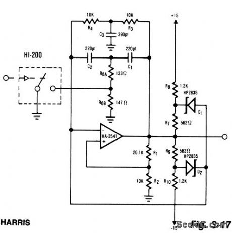
The proliferation of industrial and computerized equipment containing programmable memory has increased the need for reliable recording media.The magnetic tape medium is presently one of the most widely used methods. The primary component of any magnetic recording mechanism is the write mechanism. The concept of the write generator is very basic. The digital input causes both a change in the output amplitude, as well as a change in frequency. This type of operation is accomplished by altering the value of a resistor in the standard twin-tee oscillator. A HI-201 analog switch was used to facilitate the switching action. The effect of the external components on the feedback network requires R6A and R6B to be much smaller than would normally have been expected when using the twin-tee feedback scheme. (View)
View full Circuit Diagram | Comments | Reading(659)
4_2_differential_mux_MAX335
Published:2009/7/23 22:24:00 Author:Jessie

To use the MAX335 as a 4-X-2 differential mux, tie COMO through COM3 together and COM4 through COM7 together, Differential inputs will be at the source inputs as follows: (N00, N04), (N01, N05), (N02, N06), and (N03, N07). Figure 2-32 shows the serial input control at DIN required to turn on two switches to form a differential mux. CS is held low for four clock pulses; the first pulse is clocked into the fifth swith position as the second pulse is clocked into the first switch position. CS is pulled high to update the switches; ten CS is pulled low, and SCLK advances pulses to S1 and S5 positions, where CS is pulled high to update, etc. (View)
View full Circuit Diagram | Comments | Reading(577)
10_SEC_SCS_TIMER
Published:2009/7/23 22:24:00 Author:Jessie
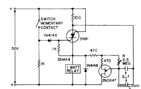
Switch applies positive pulse to gate of scs, triggering it on and thereby supplying power to relay load and ujt timing circuit. At end of timing interval, determined by R-C, timer feeds negative pulse to anode to turn off scs.- Transistor Manual, Seventh Edition, General Electric Co., 1964, p 435. (View)
View full Circuit Diagram | Comments | Reading(1366)
MAGNETIC_FILM
Published:2009/7/23 22:23:00 Author:Jessie
Circuit subtracts one sampled waveform from the next, to reduce noise disturbances by factor of 10 in equipment using strip transmission line for determining polarity reversal time of thin magnetic films to be used as switching elements in computers.-W. Dietrich and W. E. Proebster, Measuring Switching Speed of Magnetic Films, Electronics, 33:23, p 79-81. (View)
View full Circuit Diagram | Comments | Reading(528)
LINEAR_SCALE_FET_TIMER
Published:2009/7/23 22:23:00 Author:Jessie
Operation com pares to that of one-shol mvbr.Q3 is normally on and C1 is charged. When S1 is closed, Q2 and Q3 turn off. Q3 remains off until charge on C1 decreases to point where Q2 is turned on sufficiently to make Q3 con duct, Q2 here acts as voltage-variable re sistor.-Texas Instruments Inc., Transistor Circuit Design, McGraw-Hill, N.Y., 1963, p 519. (View)
View full Circuit Diagram | Comments | Reading(647)
Ultra_low_power_FM_radio_receiver
Published:2009/7/23 22:23:00 Author:Jessie
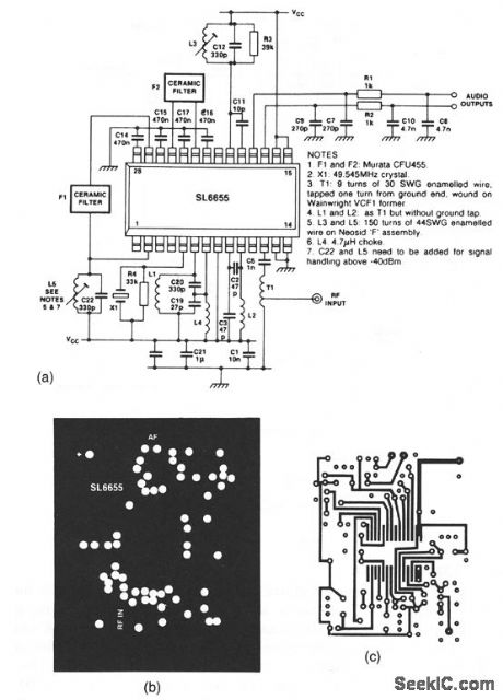
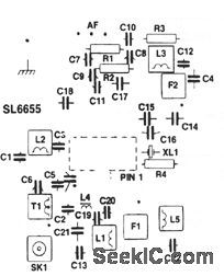
The SL6655 shown in this circuit is a single-chip RF amplifier/mixer/oscillator/IF amplifier/detector,operating with a 0.95-to 5-V Supply at a typicalcurrent of 1 mA.Typical sensitivity is 250 nV, with atypical audio output of 12 mV(rms).The circuit can operate at frequencies up to 100 MHz. Circuit values for 50-MHz operation are shown.Typical surface-mount construction details areshown in Figs. 2-34B(ground plane),2-34C(copper track),and 2-34D(component overlay)(all 1:1). (View)
View full Circuit Diagram | Comments | Reading(977)
Positive_variable_voltage_reference_VSUBOUT_SUB_is_lower_than_reference_zener
Published:2009/7/23 22:23:00 Author:Jessie
This circuit is suited for high-precision extended-temperature service, if V+ is reasonably constant (Because IZ does depend on V+). R1 through R4 are chosen to provide optimum zener current for minimum zener temperature coeffi-cient (TC), and to minimize error of Ibis. (View)
View full Circuit Diagram | Comments | Reading(518)
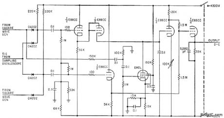
UNITY_GAIN_VIDEO_SAMPLING_AMPLIFIER
Published:2009/7/23 22:22:00 Author:Jessie
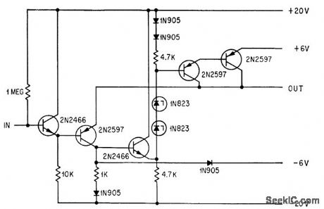
Five-transistor amplifier delivers high bidirectional current, with bandwidth of 10 Mc, for amplifying incoming radar or other pulse prior to binary conversion.-A. Hakimoglu and R. D. Kulvin, Sampling Ten Million Words a Second, Electronics, 37:6, p 52-57. (View)
View full Circuit Diagram | Comments | Reading(503)
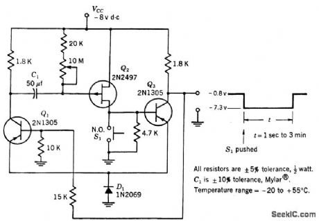
START_STOP_CONTROL
Published:2009/7/23 22:22:00 Author:Jessie

Low-cost transistor arrangement controls four precision timers used for simultaneous measurement of lime interval of four integrating circuits. Time between first digital output pulse and firing of circuit is determinable within 0.01%.-F. W. Kear, Tests Show Control is Key to Timer Accuracy, Electronics, 33:27, p 62. (View)
View full Circuit Diagram | Comments | Reading(859)
| Pages:1096/2234 At 2010811082108310841085108610871088108910901091109210931094109510961097109810991100Under 20 |
Circuit Categories
power supply circuit
Amplifier Circuit
Basic Circuit
LED and Light Circuit
Sensor Circuit
Signal Processing
Electrical Equipment Circuit
Control Circuit
Remote Control Circuit
A/D-D/A Converter Circuit
Audio Circuit
Measuring and Test Circuit
Communication Circuit
Computer-Related Circuit
555 Circuit
Automotive Circuit
Repairing Circuit