Amplifier Circuit
VOLTAGE_FOLLOWER_AMPLIFIER_FOR_SIGNAL_SUPPLY_OPERATION
Published:2009/7/3 5:25:00 Author:May | From:SeekIC
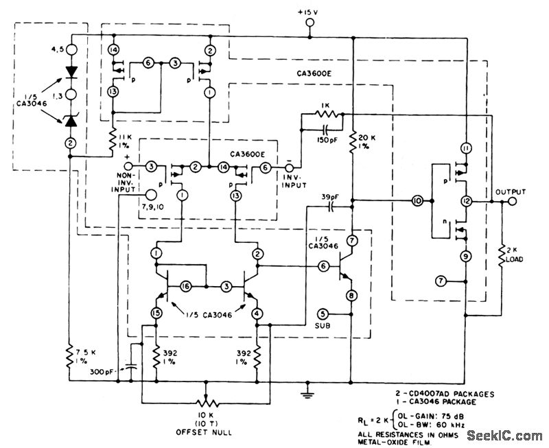
This unity-gain follower amplifier has a CMOS p-channel input, an npn second-gain stage, and a CMOS inverter output. The IC building blocks are two CA3600E's (CMOS transistor pairs) and a CA3046 npn transistor array. A zener-regulated leg provides bias for a 400-μA p-channel source, feeding the input stage, which is terminated in an npn current mirror. The amplifier voltage-offset is nulled with the 10-KΩ balance potentiometer. The second-stage current level is established by the 20-KΩ load, and is selected to approximately the first-stage current level, to assure similar positive and negative slew rates. The CMOS inverter portion forms the final output stage and is terminated in a 2-KΩ load, a typical value used with monolithic op amps. Voltage gain is affected by the choice of load resistance value. The output stage of this amplifier is easily driven to within 1 mV of the negative supply voltage.
Reprinted Url Of This Article:
http://www.seekic.com/circuit_diagram/Amplifier_Circuit/VOLTAGE_FOLLOWER_AMPLIFIER_FOR_SIGNAL_SUPPLY_OPERATION.html
Print this Page | Comments | Reading(3)

Article Categories
power supply circuit
Amplifier Circuit
Basic Circuit
LED and Light Circuit
Sensor Circuit
Signal Processing
Electrical Equipment Circuit
Control Circuit
Remote Control Circuit
A/D-D/A Converter Circuit
Audio Circuit
Measuring and Test Circuit
Communication Circuit
Computer-Related Circuit
555 Circuit
Automotive Circuit
Repairing Circuit
Code: