
Circuit Diagram
Index 1091
MAGNETOSTRICTIVE_DELAY_LINE_AMPLIFIER
Published:2009/7/23 22:56:00 Author:Jessie
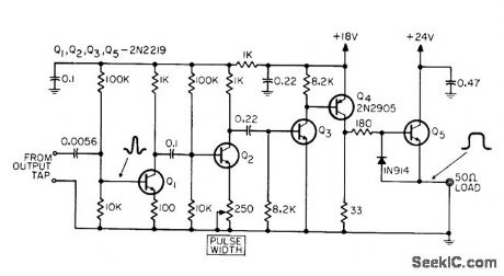
Used to reshape output signal of delay line used as 12-event serializer. Q3 clips two negative peaks of signal and Q4 fattens pulse. Pulse width control adjusts gain of Q2 to vary pulse width.-R. P. Rufer, How to Measure Simultaneous Events with Magneto-strictive Delay Lines, EEE, 14:5, p 44-49. (View)
View full Circuit Diagram | Comments | Reading(737)
PROGRAMMER_FOR_SCIENTIFIC_CALCULA_TOR
Published:2009/7/5 20:55:00 Author:May
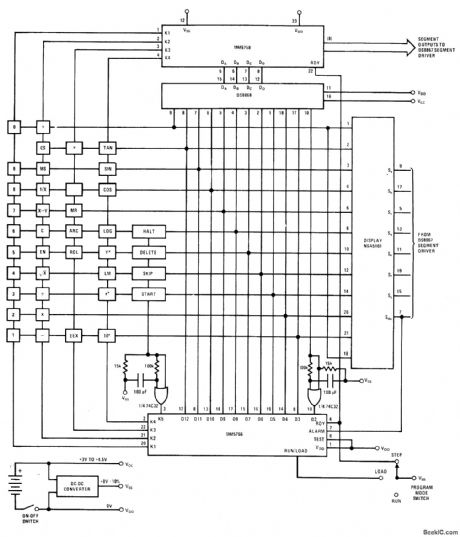
National MM5766 dynamic key sequence programmer can be added to MM5758 scientific calculator chip to provide learn-mode programmability. Cirouit memorizes any combination of key entries up to 102 characters while in load mode, then automatically plays back programmed sequence as often as desired in run mode. Halt key programs variable data entry points at which control is temporarily returned to operator in run mode.- MOS/LSl Databook, National Semiconductor, Santa Clara, CA, 1977, p 8-76-8-79. (View)
View full Circuit Diagram | Comments | Reading(731)
Digitally_controlled_dual_tracking_regulator
Published:2009/7/23 22:56:00 Author:Jessie
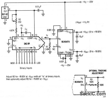
This circuit provides balanced output voltages that can be set by binary inputs applied to the DAC. Outputs vary between 0 and± 19.92 V at loads of ±200 mA.
(View)
View full Circuit Diagram | Comments | Reading(538)
HYBRID_GERMANIUM_BOXCAR
Published:2009/7/23 22:18:00 Author:Jessie
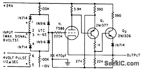
Provides time selection and storage of waveforms, as required for radar mti, sensing elements of tracking radars, and gated agc. Power drain is negligible except for 7586 nuvistor filament power of about 1 W.-A. G. Lloyd, Half-Bridge Inverter Provides Economical Three-Phase Power, Electronics, 34:37, p 62-65. (View)
View full Circuit Diagram | Comments | Reading(511)
CONSTANT_BANDWIDTH_AMPLIFIER
Published:2009/7/5 20:54:00 Author:May

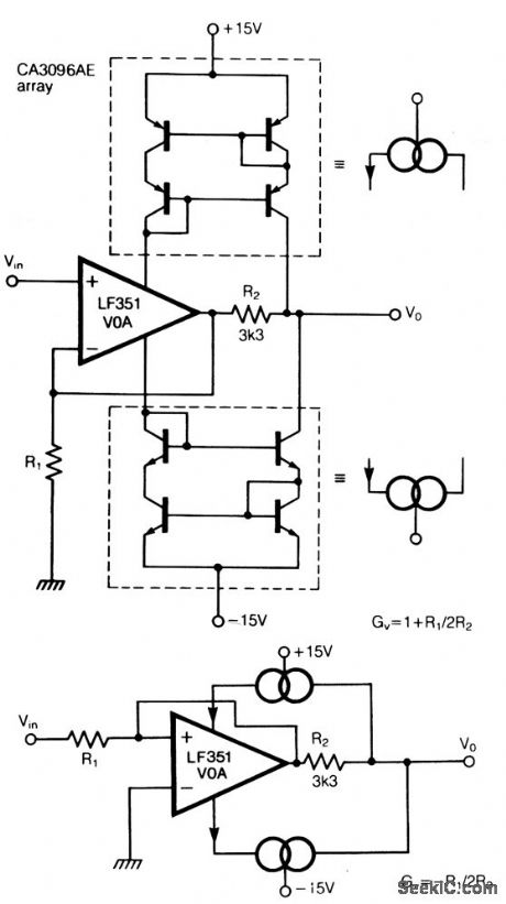
The traditional restriction of constant gainbandwidth products for a voltage amplifter can be overcome by employing feedback around a current amplifier. Two current mirrors, constructed from transistors in a CA3096AE array, effectively turn the LF351 op amp into a current amplifter. Feed-back is then applied by using R2 and R1, turning the whole circuit into a feedback voltage amplifier with a noninverting gain of G of 1 + R1 /2R2.
Using the values shown, a constant bandwidth of 3.5 MHz is obtained for all voltage gains up to and beyond 100 at 10 V pk-pk output, equivalent to a gain-bandwidth product of 350 MHz from an op amp with an advertised unity gain-bandwidth of 10 MHz. An inverting gain conftguration is also possible (see Fig. 2) where G = R1/2R2. Slewing rates are signiftcantly improved by this approach; even a 741 can manage 100 V μs under these conditions since its output is a virtual earth. However, because the new conftgurations use current feedback to achieve bandwidth independence, an output buffer should be added for circuits where a significant output current is required.
(View)
View full Circuit Diagram | Comments | Reading(708)
Livestock guardrail disconnection alarm wireless FM receiver circuit
Published:2011/8/1 2:37:00 Author:Christina | Keyword: Livestock, guardrail, disconnection, alarm, wireless, FM, receiver
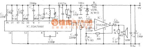
This receiver can be used with the livestock guardrail disconnection alarm wireless transmitter circuit, you can install it in the duty room or carry by the monitor staff, if the guardrail is disconnected, it will receive the FM signal (88 ~ 108MHz), the receiver speaker will send out the sound of animals. The circuit is as shown in the figure. The FM receiver uses one piece of FM ASIC TDA7010T as the core. The receiving range is 88~108MHz, and the receiving range is corresponding with the transmitting frequency. The parallel resonant circuit is composed of the L1, C8 and C9, and it can be used to adjust or track the transmitting frequency.
(View)
View full Circuit Diagram | Comments | Reading(1842)
DISK_FILE_DECODER
Published:2009/7/5 20:52:00 Author:May

Provides preconditioning of readback data from disk or drum files by using NE592 video amplifier coupled to 8T20 bidirectional mono MVBR through low-pass filter and second 592 serving as low-noise differentiator/amplifier. Mono provides required output pulses at zero-crossing points of differentiator. Designed for reading 5-MHz phase-encoded data.- Signetics Analog DataManual, Signetics, Sunnyvale, CA, 1977, p708-710. (View)
View full Circuit Diagram | Comments | Reading(1267)
CURRENT_SHUNT_AMPLIFIER
Published:2009/7/5 20:52:00 Author:May
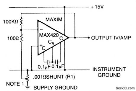
This circuit measures the power-supply current of a circuit without really having a currentshunt resistor: R1 is only 3 cm of #20 gauge copper wire. A length of the power distribution wiring can be used for R1. The MAX420's CMVR includes its own negative power supply; therefore, it can both be powered by and measure current in the ground line. (View)
View full Circuit Diagram | Comments | Reading(891)
TEST_TONES
Published:2009/7/5 20:50:00 Author:May
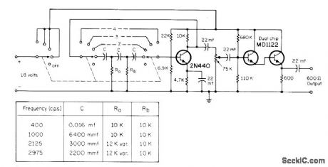
Provides preset frequencies of 400.1000.2125. and 2975 Hz Circuit consists of RC phase-shift oscillator driving Darlington emitter-follower that provides high-impedance load for osciIlator and stable 600- ohm output impedance.-s Kelly. A Simple Audio Test Oscillator.CQ1 Oct. 1970. p 50.and 90. (View)
View full Circuit Diagram | Comments | Reading(631)
DOUBLER_FOR_1_Hz_TO_12_MHz
Published:2009/7/5 20:49:00 Author:May

Simple arrangement of EXCLUSIVE-OR,mono,and hex Inverter ICs ρrovides extremely accurate frequency doubling in digital systems, along with waveform symmetry. Article gives design equation Series inverters create about 120 ns of .delay.-V. Rende, Frequency Doubler Operates from 1 Hz to 12 MHz, EDN Magazine, Aug. 20, 1976,p 85. (View)
View full Circuit Diagram | Comments | Reading(2361)
16-channel remote control circuit (T998C)
Published:2011/8/1 2:25:00 Author:Christina | Keyword: 16-channel, remote control
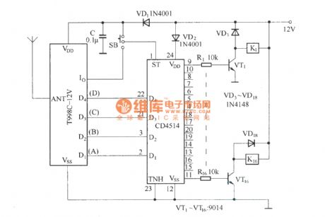
As the figure shows, the 16-channel remote control circuit (T998C) is composed of the T998C-12 V receiving module and the four-sixteen-channel decoder CD4514. This circuit can be used as the latched output and the unlatched output, the SB is the switch. When the SB is connected with the VDD, the circuit is in the latched output state, the sixteem output ports are not controlled by the Io output state; when the SB is connected with the Io output port, the circuit is in the unlatched output state, the sixteem output ports are controlled by the Io output state.
When you are using this 16-channel remote control receiving circuit, you must follow the binary-decimal encoding mode to code, and you also need to follow the coding table.
(View)
View full Circuit Diagram | Comments | Reading(3714)
1_50_kHz_SINE_WAVE
Published:2009/7/5 20:43:00 Author:May
Uses unijunction transistor as negative resistance in simple RLC circuit, Maximum output with good waveform is about 200 mV. Exact frequency depends on values used for L and C.-R. P. Hart. Simple SineWave Oscillator, Wireless World. July 1976. p 34. (View)
View full Circuit Diagram | Comments | Reading(1314)
INITIALIZING_CMOS_STORAGE
Published:2009/7/5 20:42:00 Author:May
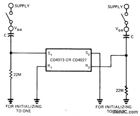
Simple RC circuit initializes all storage elements (flip-flops, registers, and counters) of CMOS system to all 1s (switch at left) or all 0s (switch at right) when power supply is turned on. For most CMOS storage elements, 30 pF for C ensures setting or resetting when power is applied by closing switch. If power supply is turned on while supply line is directly connected,C should be 1000 to 1500 pF Article also shows how to get set or reset function after initialization by uslng pairof CD4016A or CD4066A transmission gates,-o,Bismarck,A Simple Method for lnitiaizing CMOS Storage Elements,EDN Magazine, Feb.20,1974.p83 (View)
View full Circuit Diagram | Comments | Reading(843)
110_MHz_ON_SEVENTH_OVERTONE
Published:2009/7/5 20:41:00 Author:May
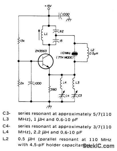
Requires only one doubler for use in 220-MHz amateur band Series-resonant traps are at frequencies of undesired lower modes.-H. Olson、 Frequency Synthesizer for 220 MHz,Ham Radio,Dec .1974,p 8-14. (View)
View full Circuit Diagram | Comments | Reading(496)
BASIC_THYRATRON_TIMER
Published:2009/7/23 22:16:00 Author:Jessie

Is not completely linear, partly because of contact potential in grid circuit, but nonlinearity errors are usually less than 3% up to about 60 sec.-R. L. Ives, Timer Made More Linear, Electronics, 32:5, p 66-69. (View)
View full Circuit Diagram | Comments | Reading(883)
1000_Hz_WITH_ONE_CHIP
Published:2009/7/5 20:39:00 Author:May
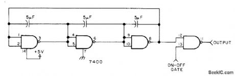
Quad NAND gate gives sawtooth output waveform at 800 to 1000 Hz for driving other TTL circuits.-Circuits. 73 Magazine. June 1977.p 49 (View)
View full Circuit Diagram | Comments | Reading(510)
Bistable switch control circuit composed of the T996/998C
Published:2011/8/1 2:04:00 Author:Christina | Keyword: Bistable, switch control circuit

The T996 component is designed as the SAW type wireless remote control launch component with the digital coding circuit, the internal circuit structure of it is the same as the CS900, but it uses the PT2262 digital coding circuit. Also it is designed as the four-channel remote control transmitter, the transmitting frequency is 418MHz. The T998 component is designed as the radio receiver device that can be used with the T996, the internal circuit is the same as the CS902, but the T998 has the digital decoding circuit PT2272.
The bistable switch control circuit which is composed of the T998C-6V and the dual D flip-flop trigger is as shown in figure (a). The four output ports D1~D4 of the T998C-6V control the turn of the four bistable flip-flops respectively to achieve the on-off of the channels.
(View)
View full Circuit Diagram | Comments | Reading(637)
BATTERY_BACKUP
Published:2009/7/5 20:36:00 Author:May
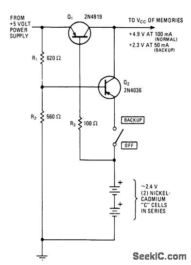
Delivers 2.3 V to microprocessor memory automatically in event of supply failure, to prevent loss of data. On standby, batteries receive charge of about 20 mA through R3 and Q1. When power supply fails, Q1 isolates it from load and Q2, conducts to provide changeover to battery power. Standby switch (optional) permits defeating battery backup.-R.N. Bennett, 2.4-V Battery Backup Protects Microprocessor Memory, Electronics, Feb. 3, 1977, p 109; reprinted in Circuits for Electronics Engineers, Electronics, 1977, p 304. (View)
View full Circuit Diagram | Comments | Reading(0)
FREE_RUNNING_HIGH_VOLTAGE_SAWTOOTH_GENERATOR
Published:2009/7/23 22:56:00 Author:Jessie

When power is applied, gale-turnoff scr triggers and applies 400 V to C1.When voltage across C1 rises above avelanche voltage of D1, GTO turns off and C1 discharges until scr conducts again.-D. R. Grafham, Now the Gate Turnoff Switch Speeds Up D-C Switching, Electronics, 37:12, p 64-71. (View)
View full Circuit Diagram | Comments | Reading(1340)
DOUBLING_100_MHz
Published:2009/7/5 20:35:00 Author:May
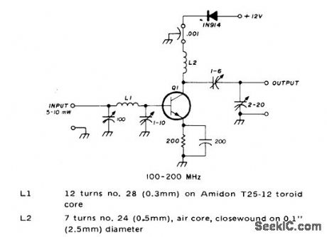
Recommended for use with VHF/UHF converters having inputs of 90 to120 MHz .Diode in series with power suρply prevents damage if the polarity is reversed.-J.Reiset, VHF/UHF Techniques,Ham Radio, March 1976,p 44-48. (View)
View full Circuit Diagram | Comments | Reading(470)
| Pages:1091/2234 At 2010811082108310841085108610871088108910901091109210931094109510961097109810991100Under 20 |
Circuit Categories
power supply circuit
Amplifier Circuit
Basic Circuit
LED and Light Circuit
Sensor Circuit
Signal Processing
Electrical Equipment Circuit
Control Circuit
Remote Control Circuit
A/D-D/A Converter Circuit
Audio Circuit
Measuring and Test Circuit
Communication Circuit
Computer-Related Circuit
555 Circuit
Automotive Circuit
Repairing Circuit