
Circuit Diagram
Index 1064
INPUT_BUFFER_FOR_PREAMP
Published:2009/7/6 1:27:00 Author:May
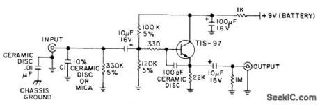
Used between cartridge and preamp of each stereo channel to make comparison testing of phonograph preamps more nearly independent of cartridge and cable capacitances. Buffer terminates cartridge in 47K in parallel with 01. Buffer can then serve as sonic reference for comparison with preamps for which input impedance is un known. Article tells how to determine correct value of C1 for cartridge used and covers preamp test procedures in detail.-T. Holman, New Tests for Preamplifiers, Audio, Feb. 1977, p 58, 60, 62, and 64. (View)
View full Circuit Diagram | Comments | Reading(703)
RIAA_PREAMP
Published:2009/7/6 1:26:00 Author:May
Low-noise circuit (below -70 dB referred to 5-mV input from pickup) has high overload capability and low distortion (below 0.05% intermodulation at 2 VRMS output}. Arrangement of first stage gives improved transient reponse over usual feedback pair. Second stage provides gain of 10.-S. F. Bywaters, RIAA-Equalized Pre-Amplifier, Wireless World, Dec. 1974, p 503. (View)
View full Circuit Diagram | Comments | Reading(1220)
SCRATCH_FILTER
Published:2009/7/6 1:25:00 Author:May

Provides passband gain of 1 and corner frequency of 10 kHz for rolling off excess high-frequency noise appearing as hiss, ticks, and pops from worn records. Design procedure is given.- Audio Handbook, National Semiconductor, Santa Clara, CA, 1977, p 2-49-2-52. (View)
View full Circuit Diagram | Comments | Reading(1378)
RUMBLE_SCRATCH_FILTER
Published:2009/7/6 1:24:00 Author:May

Used after pre-amp in high-quality audio system to improve reproduction of phonograph records. Two-pole Butterworth design has switchable breakpoints providing any desired degree of filtering.- Signetics Analog Data Manual, Signetics, Sunnyvale, CA, 1977, p 638-639. (View)
View full Circuit Diagram | Comments | Reading(1925)
NEW_RIAA_NETWORK
Published:2009/7/6 1:24:00 Author:May
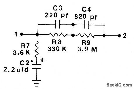
Values of R7 and C2 have been changed as shown in standard net-work for phonograph playback equalization. Tantalum electrolytic rated at least 20 V is recommended for C2. Network can also be used as inverse RIAA equalizer for testing preamps, with signal applied to terminal 2 and output to preamp taken from terminal 1. New standard extends playback equalization to 20,000 Hz and specifies that equalization be 3 dB down from previous standard at 20 Hz, with rolloff at 6 dB per octave below 20 Hz.-W. M. Leach, New RIAA Feedback Network, Audio, March 1978, p 103. (View)
View full Circuit Diagram | Comments | Reading(784)
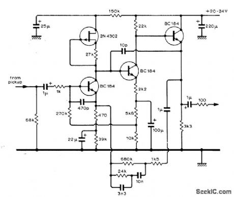
STEREO_MAGNETIC_PICKUP_PREAMP
Published:2009/7/6 1:23:00 Author:May
Single Sprague ULN-2126A IC accepts low impedance of magnetic cartridge and provides up to 2-W output power for driving commercial stereo power amplifier. Circuit includes balance control and all tone controls along with ganged volume control. Values shown give proper equalizatioan for playback of records.-E. M. Noll, “Linear IC Principles, Experiments, and Projects,” Howard W. Sams, Indianapolis, IN, 1974, p 237 and 242. (View)
View full Circuit Diagram | Comments | Reading(766)
MAGNETIC_CARTRIDGE_PREAMP
Published:2009/7/6 1:22:00 Author:May
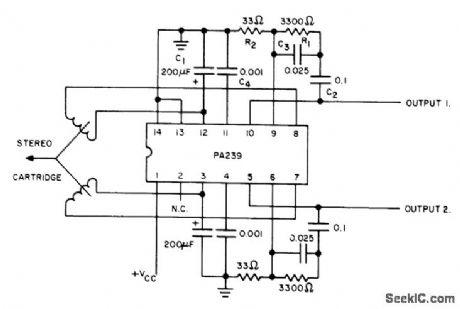
Uses Signetics PA239 dual low-noise amplifier designed specifically for low-level low-noise applications. Stereo channel separation at 1 kHz is typically 90 dB, and total harmonic distortion without feedback is 0.5%. Circuit matches amplifier response with RIAA recording characteristic. Supply voltage can be between 9 and 15 V at 22 mA. Article gives design equations.-A. G. Ogilvie, Construct a Magnetic-Cartridge Preamp, Audio, June 1974, p 40 and 42. (View)
View full Circuit Diagram | Comments | Reading(871)
PLL_WITH_IC_TIMER
Published:2009/7/6 1:18:00 Author:May

Uses 2240 programmable timer/counter as combination voltage-con-trolled oscillator and frequency divider, with CMOS analog switches serving as sample-and-hold phase detectors. Incoming reference frequency is amplified and limited by CMOS inverter, then integrated into reference triangle waveform by R9-C2. Triangle is sampled by S1 and S2 whieh with CH1 and CH2 form cascaded sample-and-hold network that holds only last instantaneous voltage on CH1 as error voltage. This error is amplified by FET-input 3140 opamp A2 for driving pin 12 of 2240 timer as correction voltage, to establish lock. Reference and output frequencies need not have direct harmonic (View)
View full Circuit Diagram | Comments | Reading(1817)
DIGITAL_CONTROL_OF_PHASE_ANGLE
Published:2009/7/6 1:16:00 Author:May

Circuit transforms 5-bit digital control word into phase angle over full range. Resolution is proportional to length of control word. Developed for stage lighting control. Z1C serves as clock oscillator that is periodically synchronized with zero crossings of AC line; R1 and C1 set clock frequency, which for 5-bit control word must be 64 times line frequency or 3.84 kHz. Load requirements determine choice of triac for Q4. Required signal for generating triac drive is produced by D1-D4 and Q1.-R. Tenny, Circuit Provides Digital Phase Control of AC Loads, EDN Magazine. Oct. 5, 1977, p 99-101. (View)
View full Circuit Diagram | Comments | Reading(2260)
FASTER_PHASE_LOCK
Published:2009/7/6 1:15:00 Author:May

Circuit was developed to reduce the normally long acquisition time of phase-locked loops when measuring frequency of short signal bursts. Synchronization of VCO to input phase allows correction pulses to be developed in correct polarity only, to give lockup time less than 10 cycles of input when using idling frequency of 12 kHz for VCO. Input signals are compared to those of VCO at EXCLUSIVE-OR gate A. Gating of error pulses by gate F and flip-flop G-H allows I or J to drive current pulses of correct polarity into C1. Voltage correction on C1, controlled by values of R2 and R3, is proportional to width of error pulses. Article covers circuit operation in detail.-R. Bohlken, A Synchronized Phase Locked Loop, EDN Magazine, March 20, 1973, p 84-85. (View)
View full Circuit Diagram | Comments | Reading(766)
VOLTAGE_FEEDBACK
Published:2009/7/6 1:14:00 Author:May
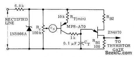
Used when quantity to be sensed is isolated varying DC voltage es such as output of tachometer. Operating point is determined by setting of RC. Output of voltage feedback circuit goes to thyristor in series with load.-D. A. Zinder, Unijunction Trigger Circuits for Gated Thyristors, Motorola, Phoenix, AZ, 1974, AN-413, p 4. (View)
View full Circuit Diagram | Comments | Reading(694)
SHIFTING_AND_SQUARING
Published:2009/7/6 1:13:00 Author:May
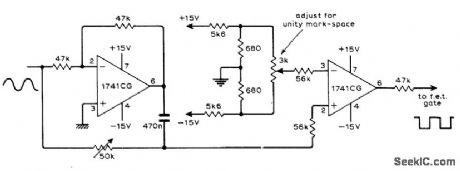
Circuit uses two opamps to derive phase-shifted reference square wave and DC output signal of phase-sensitive detector from same sine-wave signal source. Article gives theory of operation and waveforms for various operating conditions.-G. B. Clayton, Experiments with Operational Amplifiers, Wireless World, July 1973, p 355-356. (View)
View full Circuit Diagram | Comments | Reading(649)
DPSK_ON_DSBSC
Published:2009/7/6 1:12:00 Author:May
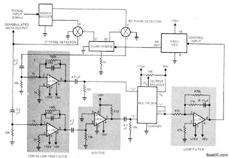
Differential phase-shift keyed double-sideband suppressed-carrier signal is demodulated by reinsertion of missing carrier, using synchronous or coherent detection. Receiver input signal is multiplexed by locally generated carrier, accurately controlled in frequency and phase. This is followed by low-pass filtering. Demodulation at output is by frequency/phase controlled loop that automatically locks local oscillator in frequency and phase to received vestige of carrier. This extracts phase information from modulated signal. Power divider is BF Associates H22, quad hybrid is Merrimac Research QHT-2, 0°and 90° phase detectors are Relcom M6A, and multiplier is Analog Devices 4281. Article covers theory and operation of circuit in detail.-R. Hennick, Demodulate DPSK Signals Coherently Using a Costas Phase-Lock Loop, EDN Magazine, July 1, 1972, p 44-47. (View)
View full Circuit Diagram | Comments | Reading(1647)
PLL_LOST_LOCK_INDICATOR
Published:2009/7/6 1:11:00 Author:May

Developed for use with phase-locked loop to indicate both acquisition and loss of lock. Based on concept that lock exists as long as static-phase error is less than 90°. Uses quad opamp package such as RC4136, with A4 feeding retriggerable one-shot; output of one-shot is low when lock exists. When lock is lost, output of one-shot immediately goes high and remains high until lock is reacquired plus time duration of one-shot. Developed for use in systems where certain processes must be interrupted immediately upon loss of lock.-J. C. Hanisko, PLL Lock Indicator Uses a Single IC, EDN Magazine, Oct. 5, 1976, p 104. (View)
View full Circuit Diagram | Comments | Reading(996)
LOSS_OF_LOCK_MONITOR
Published:2009/7/6 1:10:00 Author:May

Modified digital phase-locked loop includes second phase detector that provides alarm signal when loop gets out of lock. Output may also be used to disable other circuits. Voltage-controlled multivibrator VCO, operating at 4 times desired clock frequency, drives two-stage switch-tailed ring counter that provides two-phase internal clock signals A and B for detectors. Article descirbes operation of circuit and give timing digrams.-C.A. Herbst, Digital Phase-Locked Loop with Loss-of-Lock Monitor, EDN|EEE magazine, Oct. 15, 1971, p, 64-65. (View)
View full Circuit Diagram | Comments | Reading(2407)
Basic_function_tests
Published:2009/7/23 21:43:00 Author:Jessie

Figures 2-C and 2-D show the typical application circuit and pin configuration/ logic, respectively, for the MAX326/27. Test this ultra-low-leakage CMOS analog switch by applying and removing +5 V to the channel-control pins, and checking that the corresponding switches open and close. Use an ohmmeter connected across the switch pins. (View)
View full Circuit Diagram | Comments | Reading(526)
PHASE_COMPARATOR
Published:2009/7/6 1:09:00 Author:May

Signetic balanced moudulator-demodulator transistor array is connected as phase detector in which output contains term related to cosine of phase angle, Equal-frequency input signals are multiplied together by IC to produce sum and difference frequencies. Difference component becomes DC, while undesired sum component is related to phase angle, with cosine becoming 0 at 90° and having maximum positive or negaitive value at 0° and 80° respectively. Balanced modulator provides excellent conversion linearity along with conversion gain.-“Signetics Analog Date Manual,” Signetics, Sunnyvale, CA, 1977, p, 757-758. (View)
View full Circuit Diagram | Comments | Reading(4201)
Balanced_high_level_mixer
Published:2009/7/23 21:42:00 Author:Jessie
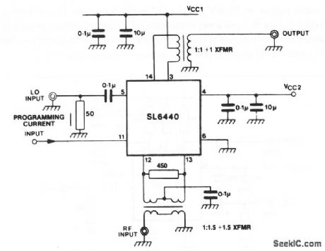
This circuit shows the SL6440 (Fig. 2-10) with a balanced input (for improved carrier leak), and balanced output (for increased conversion gain). A lower VCC can be used with this arrangement (for lower device dissipation).Conversion gain for the balanced circuit of Fig. 2-11 is equal to: Gdb 20=20 Log56.61 IP+0.0785,2RLIP.where IP is programmed current at pin 11, and RL is dc load resistance. (View)
View full Circuit Diagram | Comments | Reading(1076)
FRANKLIN_SUPERREGENERATIVE_RECEIVER
Published:2009/7/23 21:42:00 Author:Jessie

Has low sensitivity to impulse noise, wide dynamic range, high gain, and flexibility, since quench oscillator components are at r-f potential and feedback adjustments more easily made. Oscillates at 27 Mc as modified Hartley with interelectrode capacitances tuned by L1, and also oscillates at 25-kc quench frequency. Provides large decrease in plate current when signal arrives.-S. J.Neshyba and F. E. Brooks, Jr., Stable Receiving Circuits for Remote Control, Electronics, 31:31, p 74-76. (View)
View full Circuit Diagram | Comments | Reading(963)
0_360°PHASE_SHIFTER
Published:2009/7/6 1:09:00 Author:May

Each J202 JFET stage provides up to 180° phase shift under control of 1-megohm pot. Ganged pots give full range of control. JFETs specified are ideal for circuit be-cause they do not load phase-shift networks.- FET Databook, National Semiconductor, Santa Clara, CA, 1977, p 6-26-6-36. (View)
View full Circuit Diagram | Comments | Reading(928)
| Pages:1064/2234 At 2010611062106310641065106610671068106910701071107210731074107510761077107810791080Under 20 |
Circuit Categories
power supply circuit
Amplifier Circuit
Basic Circuit
LED and Light Circuit
Sensor Circuit
Signal Processing
Electrical Equipment Circuit
Control Circuit
Remote Control Circuit
A/D-D/A Converter Circuit
Audio Circuit
Measuring and Test Circuit
Communication Circuit
Computer-Related Circuit
555 Circuit
Automotive Circuit
Repairing Circuit