Electrical Equipment Circuit
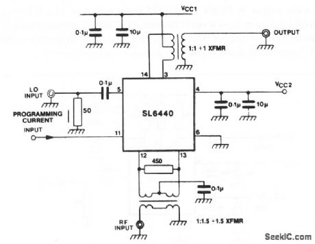
Balanced_high_level_mixer
Published:2009/7/23 21:42:00 Author:Jessie | From:SeekIC

This circuit shows the SL6440 (Fig. 2-10) with a balanced input (for improved carrier leak), and balanced output (for increased conversion gain). A lower VCC can be used with this arrangement (for lower device dissipation).Conversion gain for the balanced circuit of Fig. 2-11 is equal to: Gdb 20=20 Log56.61 IP+0.0785,2RLIP.where IP is programmed current at pin 11, and RL is dc load resistance.
Reprinted Url Of This Article:
http://www.seekic.com/circuit_diagram/Electrical_Equipment_Circuit/Balanced_high_level_mixer.html
Print this Page | Comments | Reading(3)

Article Categories
power supply circuit
Amplifier Circuit
Basic Circuit
LED and Light Circuit
Sensor Circuit
Signal Processing
Electrical Equipment Circuit
Control Circuit
Remote Control Circuit
A/D-D/A Converter Circuit
Audio Circuit
Measuring and Test Circuit
Communication Circuit
Computer-Related Circuit
555 Circuit
Automotive Circuit
Repairing Circuit
Code: