
Circuit Diagram
Index 1076
VHF_antenna_booster
Published:2009/7/23 21:56:00 Author:Jessie
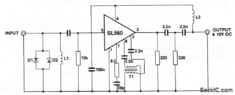
This circuit shows an SL560 amplifier connected as a wideband (40 to 260 MHz) antenna amplifier or booster suitable for any 50-Ω system. D1 and D2 are any general-purpose silicon diodes. L1 is 8 turns of #26, 1/8 intemal diameter.L2 is 20 turns of #26, 3/16 intemal diameter. T1 consists of two lengths of #34 wire approximately 6 long, twisted together (8 twists/inch) and wound on a 6-hole ferrite bead (Mullard FX1898). The circuit is powered through the coaxial cable (+10 V at the coax center, and ground at the coax outer shield), and requires about 30 mA. (View)
View full Circuit Diagram | Comments | Reading(680)
ONE_SECOND,1_kHz_OSCILLATOR
Published:2009/7/5 22:49:00 Author:May

This circuit operates as an oscillator and a timer. The 2N6028 is normally on due to excess holding current through the 100 k resistor.
When the switch is momentarily closed, the 10 μF capacitor is charged to a full 15 volts and 2N2926 starts oscillating (1.8 M and 820 pF). (View)
View full Circuit Diagram | Comments | Reading(2217)
Photoconductive_cell_amplifier
Published:2009/7/23 21:56:00 Author:Jessie

R1 depends on cell sensitivity, and should be chosen for eithermaxlmum dynamic range, Or for a desired scale factor. R2 is used tominimize outputoffset. and can be omitted in many applications. (View)
View full Circuit Diagram | Comments | Reading(692)
Basic_rnux_function_tests
Published:2009/7/23 21:56:00 Author:Jessie

Figures 2-O and 2-P shows the typical application circuit and pin configuration, respectively; for the MAX328/29. Figures 2-Q and 2-R shows the logic truth tables for the MAX328 and MAX329, respectively. This ultra-low-leakage CMOS analog mux is tested by applying and removing +5 V to the control pins, and checking that the corresponding switches open and close. Simple sine waves can be used at the analog inputs, and the op-amp output can be measured on a scope. (View)
View full Circuit Diagram | Comments | Reading(685)
CAPACITOR_TESTER
Published:2009/7/5 22:48:00 Author:May

Portable instrument measures capacitance values to 2500μF and leakage current with up to 8 V applied. Timer U1 operates as clock providing about 350 negative-going pulses per second to trigger timer U2 and unclamp test capacitor so it charges through switch-selected resistor to half of supply voltage. U2 then resets, discharging capacitor through pin 7. During charge, pin 3 of U2 is high (about 8 V) and duration of high state is directly proportional to capacitance. Resulting rectangular waveform is applied to unity-gain buffer opamp U3 that feeds meter through calibrating trimpot R6. Meter deflection is proportional to average value of rectangular output waveform and is therefore proportional to capacitance. Table gives switch functions. Mode B uses larger clock timing capacitor to permit measuring larger capacitance values, for total of10 ranges Article covers construction,calibration and use.-P. H. Mathleson, Wide-Range Capacitance Meter, Ham Radio, Feb.1978,p51-53 (View)
View full Circuit Diagram | Comments | Reading(3051)
OSCILLATOR_ADJUSTABLE_OVER_10_1_RANGE
Published:2009/7/5 22:48:00 Author:May

In this circuit, there are two feedback paths around an op amp. One is positive dc feedback which forms a Schmitt trigger. The other is a CR timing network. Imagine that the output voltage is +10V. The voltage at the noninverting terminal is +15V.
The voltage at the inverting terminal is a rising voltage with a time constant of CTRT.
When this voltage exceeds + 5V, the op amp's output will go low and the Schmitt trigger action will make it snap into its negative state. Now the output is - 10 V and the voltage at the inverting terminal falls with the time constant as before. By changing this time constant with a variable resistor, a variable frequency oscillation may be produced. (View)
View full Circuit Diagram | Comments | Reading(1306)
PARALLEL_PATH_CONTINUITY_CHECKER
Published:2009/7/23 21:56:00 Author:Jessie
Used for monitoring nonseparable parallel paths for continuity in automatic testing equipment. Current through circuit under rest is limited, to prevent damage to low-power circuits. Resistance levels for continuity checks are set at 5, 20, 100, and 1,000 ohms.-R. H. Wassum, Parallel-Path Continuity-Checking Circuit, EEE, 14:8, p 164-166. (View)
View full Circuit Diagram | Comments | Reading(648)
5_pF_TO_1μF
Published:2009/7/5 22:47:00 Author:May

Consists of an oscillator using two gates from CD4011 quad NAND gate, separated from diode rectifier by another NAND gate. Increasing oscillator frequency gives more pulses per second and higher integrated meter reading. Each meter range is linear, so value of 5-pF capacitor can be read on lowest range.Diodes are 1N34 or equivalent. R1 is 12K, and R2-R6 are 50K trimpots set to values shown in table. R7 is 5K, and R8 is 10K trimpot. B1 is 9-V transistor battery. Article covers construction and calibration with known capacitors.-E. Landefeld, Build a Simple Capacitance Meter, 73Magazine, Jan. 1978, p 164-165. (View)
View full Circuit Diagram | Comments | Reading(1197)
1000_MC_NPN_OSCILLATOR
Published:2009/7/23 21:56:00 Author:Jessie

Can deliver over 2 mw, adequate for uhf tuner, and operate at temperatures up to 200℃.-Gigacycle Oscillator, EEE,10:12, p 102. (View)
View full Circuit Diagram | Comments | Reading(1741)
POWER_SUPPLY_MONITOR
Published:2009/7/5 22:47:00 Author:May
Circuit Notes
This circuit uses a tricolor LED display to indicate acceptable and unacceptable output voltages. One to set the upper voltage limit, the other, the lower voltage limit. When the monitored voltage is above the set maximum, the LED display turns red. Yellow turns on for voltages below the set minimum, and green turns on for voltages between the high and the low settings. The circuit does not need a separate power supply. It is powered by the voltage it monitors.The circuit can be adapted to monitor voltage differences between two power supplies. Should the monitored voltages differ by more than a set value, a visual or an audible alarm would warn the operator about the difference.The circuit can also be modified for remote monitoring and the use of a separate power supply. (View)
View full Circuit Diagram | Comments | Reading(0)
AGC_WITH_SQUELCH_CONTROL
Published:2009/7/5 22:47:00 Author:May

Automatic gain control is a very useful feature in a number of audio amplifier circuits:tape recorders,telephone speaker phones,communication systems and PA systems.This circuit consists of a HA-5144 quad op amp and a FET transistor used as a voltage-controlled resistor to implement an AGC circuit with squelch control.The squelch function helps eliminate noise in communications systems when no signal is present and allows remote hands-free operation of tape recorder systems.Amplifier A1 is placed in inverting-gain T configuration in order to provide a fairly wide gain range and a small signal level across the FET. The small signal level and the addition of resistors R5 and R6 help reduce nonlinearities and distortion.Amplifier A2 acts as a negative peak detector to keep track of signal amplitude.Amplifier A3 can be used to amplify this peak signal if the cutoff voltage of the FET is higher than desired.Amplifier A4 acts as a comparator in the squelch control section of the circuit,When the signal level falls below the voltage set by R10,the gate of the FET is pulled low-turning it off completely-and reducing the gain to 2.4.Theoutput A4 can also be used as a control signal in applications,such as a hands-free tape recorder system.
(View)
View full Circuit Diagram | Comments | Reading(4171)
ELECTROEXPLOSIVE_PULSER
Published:2009/7/23 21:55:00 Author:Jessie
Used in determining energy required to fire 50% of devices being tested. Uses thyratron as pulse generator, transistor for pulse shaping, and power transistor as linear amplifier to give either constant-current or constant-voltage pulses over wide range (0 to 10 v or 0 to 10 amp at durations of 100 to 1,000 microsec).-L. A. Rosenthal, Generator Delivers Constant Current or Voltage Pulses, Electronics, 33:38, p 82-84. (View)
View full Circuit Diagram | Comments | Reading(698)
Linear Voltage Regulating Circuit of LTC1422
Published:2011/7/24 7:07:00 Author:Michel | Keyword: Linear Voltage, Regulating Circuit
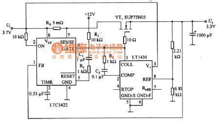
Picture 55 is linear voltage regulating circuit of LTC1422.When the input voltage Ui is added to the circuit,feet 2 of LTC1422 is high potential and feet 6 is low potential and the absorbing current is 10mA.At the time,VT1 stops and the output U。is zero.The phase input end (feet 1) voltage in LTC1422 comparator is zero.The output voltage in the comparator is lower than 1.232V reference voltage,thus feet 5 remains low PWL.After a timing cycle,the feet 6 of LTC1422 provides 1OμA for VT1.12V voltage is connected to feet 6 via R1 and it charges C1 with 1.2mA current via R2.R2 and C1 drops slowly and VT1 gate rises to limit impulsing current. (View)
View full Circuit Diagram | Comments | Reading(422)
Model_control_receiver
Published:2009/7/23 21:55:00 Author:Jessie

This circuit shows the ZN414Z (Fig. 2-14A) used as an IF amplifier for a 27-MHz superhet receiver, such as those used in model remote-control systems. (View)
View full Circuit Diagram | Comments | Reading(854)
400_Hz_LED_OPAMP_SlNE_WAVE
Published:2009/7/5 22:47:00 Author:May

Uses LEDs as nonlinear- resistance diodes in Wien-bridge configuration with opamp operating from 15-V supply. Circuit will operate over wide range of other frequencies if values of R and C are changed. R5 adjusts output amplitude from 10 to 20 V P-P. Total harmonic distortion is 15%.-W. G. Jung, LED's Do Dual Duty in Sine-Wave Oscillator, EDN Magazine, Aug. 20, 1976, p 84-85. (View)
View full Circuit Diagram | Comments | Reading(742)
Dual-symmetric regulated power supply circuit composed of RC4194TK and RC4194D
Published:2011/5/10 1:10:00 Author:Rebekka | Keyword: Dual-symmetric regulated power supply

Dual-symmetric regulated power supply circuit composed of RC4194TK and RC4194D. (View)
View full Circuit Diagram | Comments | Reading(1071)
TUNNEL_DIODE_TRANSMITTER
Published:2009/7/23 21:55:00 Author:Jessie

Can be frequency-modulated for remote-control applications. All components are mounted on body of piston-type trimmer capacitor. Tuning range is 50 to 250 Mc.-Tuner Elements Ride Piggyback, Electronics, 35:31, p 54-56. (View)
View full Circuit Diagram | Comments | Reading(1753)
SIMPLE_TRIANGLE_SQUARE
Published:2009/7/5 22:47:00 Author:May
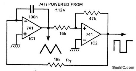
This circuit generates simultaneously, a triangle and a square waveform. It is self starting and has no latch up problems. IC1 is an integrator with a slew rate determined by CT and RT and IC2 is a Schmitt trigger. The output of IC1 ramps up and down be-tween the hysteresis levels of the Schmitt, the output of which drives the integrator.
By making RT variable, it is possible to alter the operating frequency over a 100 to 1 range. Three resistors, one capacitor, and a dual op amp is all that is needed to make a versatile triangle and square wave oscillator with a possible frequency range of 0.1 Hz to 100 kHz. (View)
View full Circuit Diagram | Comments | Reading(747)
Integrator
Published:2009/7/23 21:54:00 Author:Jessie

This circuit was originally developed to perform the mathematical operation of integration in analog computers. As shown by the frequency-response plot of Fig. 10-41B, an integrator is essentially a low-pass filter with a frequency response that decreases at 6 dB per octave. When S1 is in position 1, the amplifier is connected in unity gain, and C1 is discharged, which sets an initial condition of zero volts. With S1 in position 2, the amplifier is connected as an integrator, where the output changes in accordance with a constant times the time integral of the input. (View)
View full Circuit Diagram | Comments | Reading(1192)
C_WITH_VOM
Published:2009/7/5 22:47:00 Author:May
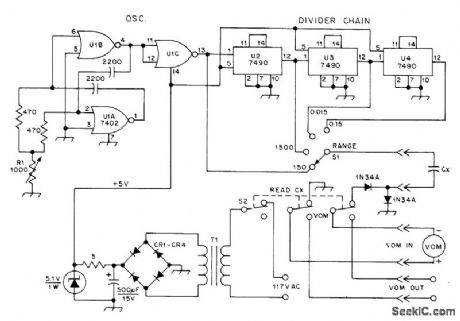
TTL-derived square-wave gen-erator U1 charges unknown capacitor CX to about 3.5 V at 285 kHz when using 150-μA scale of Heath MM-1 volt-ohm-milliammeter, to give 150-pF full-scale range. Larger values of capacitance are read by decreasing frequency with 7490 decade dividers. Use Mallory PTC401 for CR1-CR4. T1 is 6.3-VAC filament transformer. S2 restores normal VOM functions. Article gives design equations.-K. H. Cavcey, Read Capacitance with Your VOM,QST,Dec. 1975, p 36-37. (View)
View full Circuit Diagram | Comments | Reading(799)
| Pages:1076/2234 At 2010611062106310641065106610671068106910701071107210731074107510761077107810791080Under 20 |
Circuit Categories
power supply circuit
Amplifier Circuit
Basic Circuit
LED and Light Circuit
Sensor Circuit
Signal Processing
Electrical Equipment Circuit
Control Circuit
Remote Control Circuit
A/D-D/A Converter Circuit
Audio Circuit
Measuring and Test Circuit
Communication Circuit
Computer-Related Circuit
555 Circuit
Automotive Circuit
Repairing Circuit