
Circuit Diagram
Index 1079
OPTICAL_COMMUNICATION_SYSTEM
Published:2009/7/5 22:36:00 Author:May
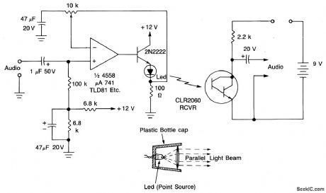
The circuit will modulate the light from the LED usmg a crystal cnicrophone or a loudspeaker output.To obtain the maximum range,the optical system must be efficient(see example),Either a convex lens or a concave mirror can be used to convert the LED output into a parallel beam.The received light is concentrated onto a sensitivephotodarlington transistor. At short range the signal across the load resistor is adequateto drive a crystal earpiece,for longer range an amplifier and a loudspeaker are needed. (View)
View full Circuit Diagram | Comments | Reading(1479)
ZJ-100VA emergency power supply circuit diagram
Published:2011/5/10 1:18:00 Author:Rebekka | Keyword: emergency power supply
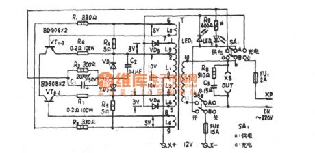
ZJ-100VA emergency power supply circuit diagram. (View)
View full Circuit Diagram | Comments | Reading(514)
Korean RE-630D Mechanical Microwave Oven Circuit
Published:2011/8/2 3:13:00 Author:Robert | Keyword: Korean, Mechanical, Microwave, Oven

The picture shows the Korean RE-630D mechanical microwave oven circuit.
The circuit in the picture is in open mode.
The ST is temperature control device. The S1 is door first interlock switch. The S2 is door second interlock switch. The S3 is door monitoring switch. The EL is oven lamp. The M1 is timing motor. The M2 is rotating plate motor. The M3 is fan motor. The T is high-voltage transformer. The C is high-voltage capacitor. The V is high-voltage diode. The MT is magnetron. The S4 is timer switch. The S5 is power selection switch. (View)
View full Circuit Diagram | Comments | Reading(2884)
Volumn control circuit diagram
Published:2011/6/23 4:23:00 Author:Rebekka | Keyword: Volumn control

Volumn control circuit diagram. (View)
View full Circuit Diagram | Comments | Reading(459)
GAS_SMOKE_DETECTOR_WITH_LATCH
Published:2009/7/5 22:36:00 Author:May

CMOS latching logic provides 2-min time delay to prevent false alarm when power is first applied to fire alarm using Taguchi TGS308 gas sensor whose conductivity increases in presence of combustible gases. Normal voltage of 3 VRMS across R4 increases to about 20 V in presence of fire. Half of 12.6-V center-tapped transformer secondary is used for 6-V supply and full 12.6 V for DC horn supply. Latch is reset manually with S1 to turn off alarm after gas level drops. Optional circuit shown can be used for automatic reset.-A, Pshaenich, Solid State Gas/Smoke Detector Systems, Motorola, Phoenix, AZ, 1975, AN-735, p 5. (View)
View full Circuit Diagram | Comments | Reading(1654)
ZERO_CROSSING_DETECTOR
Published:2009/7/5 22:34:00 Author:May

View full Circuit Diagram | Comments | Reading(0)
4-word control keyboard circuit diagram
Published:2011/5/10 1:34:00 Author:Rebekka | Keyword: 4-word control keyboard

4-word control keyboard circuit diagram. (View)
View full Circuit Diagram | Comments | Reading(702)
ZERO_CROSSING_SWITCH
Published:2009/7/5 22:34:00 Author:May

When switching loads with the aid of a thyristor, a large amount of RFI can be generated unless some form of zero crossing switch is used. The circuit shows a simple single transistor zero crossing switch. R1 and R2 act as a potential divider. The potential at their junction is about 10% of the ac voltage. This voltage level is fed, via R3, to the transistor's base. If the voltage at this point is above 0.2, the transistor will conduct, shunting any thyris-tor gate current to ground. When the line po-tential is less than about 2 V, it is possible to trigger the thyristor. The diode D1 is to re-move any negative potential that might cause reverse breakdown. (View)
View full Circuit Diagram | Comments | Reading(3914)
TJ-3-100 emergency power supply circuit diagram
Published:2011/5/10 1:34:00 Author:Rebekka | Keyword: emergency power supply
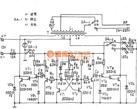
TJ-3-100 emergency power supply circuit diagram. (View)
View full Circuit Diagram | Comments | Reading(512)
1_kHz_WIEN_BRIDGE
Published:2009/7/5 22:34:00 Author:May
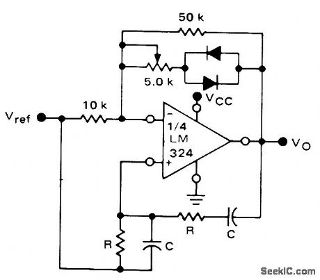
Simple circuit uses only one section of LM324 quad opamp having true differential inputs. Supply voltage range is 3-32 V. Reference voltage is half of supply voltage.Values of R and C determine frequency accord-ing to equation f = 1/6.28RC. For 16K and 0.01 μF, frequency is 1 kHz. Diode types are not criticaL- Quad Low Power Operational Amplifiers, Motorola, Phoenix, AZ, 1978, DS 9339 R1. (View)
View full Circuit Diagram | Comments | Reading(929)
ISOLATION_AND_ZERO_VOLTAGE_SWITCHING_LOGIC
Published:2009/7/5 22:33:00 Author:May
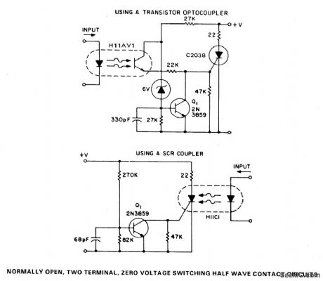
These two simple circuits provide zero voltage switching. They can be used with full wave bridges or in antiparallel to provide full wave control and are normally used to trigger power thyristors. If an input signal is present during the time the ac voltage is between 0 to 7 V, the SCR will turn on. But, if the ac voltage has risen above this range and the input signal is then applied, the transistor, Q1, will be biased to the on state and will hold the SCR and, consequently, the relay off until the next zero crossing. (View)
View full Circuit Diagram | Comments | Reading(1323)
DIGITAL_TRANSMISSION_ISOLATOR
Published:2009/7/5 22:32:00 Author:May

An optoelectronics device is used to couple a digital (TTL) signal to another system. The photodiode in the optocoupler drives an LM311 set up to produce a TTL compatible output. It is useful where grounds are not able to be connected for any reason. (View)
View full Circuit Diagram | Comments | Reading(0)
PRECISION_OSCILLATOR_TO_SWITCH_100_mA_LOADS
Published:2009/7/5 22:32:00 Author:May
View full Circuit Diagram | Comments | Reading(603)
HIGH_SPEED_PAPER_TAPE_READER
Published:2009/7/5 22:32:00 Author:May

When computer peripheral equipment is interfaced, it is convenient to work with logic signal levels. With a nominal 4V at the output dropping to -0.6V on illumination, this circuit reflects the requirements of a high-speed, paper tape optical reader system.
The circuit operates at rates of up to 1000 bits per second. It will also operate at tape translucency such that 50% of the incident light is transmitted to the sensor, and provide a fixed threshold signal to the logic circuit, all at low cost. Several circuit tricks are required. Photodarlington speed is enhanced by cascode constant voltage biasing. The output threshold and tape translucency requirements are provided for by sensing the output voltage and operating to 2000 bits per second at ambient light levels equal to signal levels. (View)
View full Circuit Diagram | Comments | Reading(601)
FREQUENCY_DIVIDER_AND_STAIRCASE_GENERATOR
Published:2009/7/5 22:32:00 Author:May

View full Circuit Diagram | Comments | Reading(2388)
WIDE_RANGE_VARIABLE_OSCILLATOR
Published:2009/7/5 22:31:00 Author:May

View full Circuit Diagram | Comments | Reading(659)
SMOKE_DETECTOR
Published:2009/7/5 22:31:00 Author:May

Battery-operated ionization-type srnoke detector uses RCA CA3130 opamp as interface for ionization chamber that provides picoampere currents. With opamp in pulsed mode (on for 20 ms of 20-s period), IC draws only 0.6 μA average instead of 600 μA.Other active components and zener, all on RCA CA3097 array, provide Low-battery monltor and horn-driver functions. When chamber detects smoke, combination of RF and D1 provides sufficient base current to keep Q3 and Q4 on.Opamp is then powered continuously, and steering diode Z1 supplies continuous current to gate of Q2 for energizing hom. Battery drain is only 5 mA in monitoring mode.-G. J. Granieri, Bipolar-MOS and Bipolar IC's Buildlng Blocks for Smoke-Detector Circuits, IEEE Transactions on Consumer Electronics, Nov. 1977, p 522-527.
(View)
View full Circuit Diagram | Comments | Reading(2271)
OSCILIATOR_WITH_QUADRATURE_OUTPUT
Published:2009/7/5 22:30:00 Author:May

View full Circuit Diagram | Comments | Reading(661)
Fronting Prescale Integrated Circuit of TD6134AF Dual Mode
Published:2011/7/22 22:51:00 Author:Michel | Keyword: Dual Mode, Fronting Prescale, Integrated Circuit


TD6134AF integrated circuit provides fronting prescaler used in low voltage power supply type digital tuned system and the working frequency maximum is 250 MHz.
First,TD6134AF Inside Circuit Block Diagram and Pins Functions
Inside circuit block diagram of TD6134AF intergrated circuit is shown as picture 1.This IC adopts 8 feet DIP structure and its pins functions and data of the intergrated circuit are shown as table.
Inside Circuit Block Diagram of TD6134AF Intergrated Circuit
Second,Typical Application Circuit of TD6134AF
The typical application circuit of TD6134AF intergrated block is shown as picture 2.
Third,TD6134AF Main Functions Because the FM frequency signal is 108 MHz and a 10.7 MHz intermediate frequency is added and the highest vibration FM is 118.7MHz.
(View)
View full Circuit Diagram | Comments | Reading(677)
HIGH_SENSITIVITY,NORMALLY_OPEN,TWO_TERMINAL,ZERO_VOLTAGE_SWITCHING,HALF_WAVE_CONTACT_CIRCUIT
Published:2009/7/5 22:30:00 Author:May
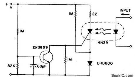
The SCR coupler circuit provides higher sensitivity toinput signals as illustrated.This allows the lower cost 4N39(H11C3)to be used with the>7 mA drive currentssupplied by the input circuit. (View)
View full Circuit Diagram | Comments | Reading(541)
| Pages:1079/2234 At 2010611062106310641065106610671068106910701071107210731074107510761077107810791080Under 20 |
Circuit Categories
power supply circuit
Amplifier Circuit
Basic Circuit
LED and Light Circuit
Sensor Circuit
Signal Processing
Electrical Equipment Circuit
Control Circuit
Remote Control Circuit
A/D-D/A Converter Circuit
Audio Circuit
Measuring and Test Circuit
Communication Circuit
Computer-Related Circuit
555 Circuit
Automotive Circuit
Repairing Circuit