
Circuit Diagram
Index 1072
SINPLE_PHASE_DETECTOR_CIRCUIT
Published:2009/7/5 23:16:00 Author:May

The operation of the circuit is like an enabled inverter, that is, the output Y=B provided A is high. If A is low, output is low (independent of the state of B). When the signals A and B or B1 are connected to the inputs A and B of this gate the output Y is a pulse train signal (shown a Y or Y1) which has a pulse duration equal to the phase difference between the two signals. The circuit is directly suitable for phase difference measurement from zero to 180°. This performance is similar to the circuits like the Exclusive OR gate used for this purpose. With this method leading and lagging positions of the signals can also be found using an AND gate. Phase difference measured along with the leading and lagging information gives complete information about the phases of the two signals between zero and 360°. (View)
View full Circuit Diagram | Comments | Reading(1058)
Shanghai Sharp R-750B Computer-Type Barbecue Microwave Oven Circuit
Published:2011/8/2 19:26:00 Author:Robert | Keyword: Shanghai, Sharp, Computer-Type, Barbecue, Microwave Oven
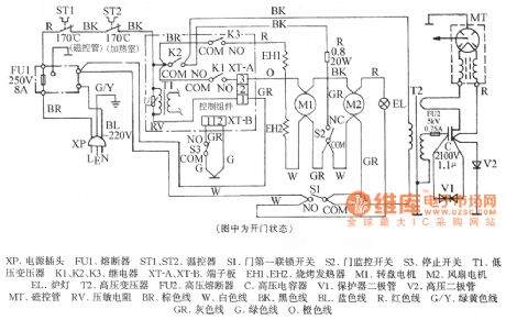
The picture shows the Shanghai Sharp R-750B computer-type barbecue microwave oven circuit.'
In the picture the XP is voltage plug. The FU1 is fuse. The ST1 and ST2 are temperature controllers. The S1 is door first interlock switch. The S2 is door monitoring switch. The S3 is stopping switch. The T1 is low-voltage transformer. The K1, K2, K3 are relays. The XT-A, XT-B are terminal board. The EH1, EH2 are barbecue heater. The M1 is rotating plate motor. The M2 is fan motor. The EL is oven lamp. The T2 is high-voltage transformer. The FU2 is high-voltage fuse. The C is high-voltage capacitor. The V1 is protector diode. The V2 is high-voltage diode. The MT is magnetron. The RV is varistor. The BR is brown wire. The W is white wire. The BK is black wire. The BL is blue wire. The R is red wire. The G/Y is green/yellow wire. The GR is gray wire. The G is green wire. The O is orange wire. (View)
View full Circuit Diagram | Comments | Reading(1984)
15_V_OR_3_V_INDICATOR
Published:2009/7/5 23:15:00 Author:May

Digi-Key LM3909N flasher/oscillator drives LED serving as ON/OFF indicator for battery-operated devices. At flash rate of 2 Hz, battery life almost equals shelf life.-C, Shaw, ON-OFF Indicator for Battery Device, QST, March 1978, p 41-42. (View)
View full Circuit Diagram | Comments | Reading(2269)
20_20000_Hz_LOW_DISTORTION
Published:2009/7/5 23:15:00 Author:May
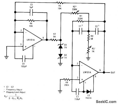
Opamp at right is driven by dquare-wave output of comparator at left, with feedback between opamps providing oscillation. Frequency range covered by tuning control R3 is determined by equalvalue capacitors C1 and C2, which range from 0.4 μF for 18-80 Hz to 0.002 μF for 4.4-20 kHz. Distortion rangesfrom 0.2% to 0.4% when 20% clipping of sine wave is provided by zeners.Both positive and negative supplies should be bypassed with 0.1-μF disk ceramic capacitors.- Easily Tuned Sine Wave Oscillators, National Semiconductor, Santa Clara, CA, 1971, LB-16. (View)
View full Circuit Diagram | Comments | Reading(600)
PHASE_SEQUENCE_DETECTOR_II
Published:2009/7/5 23:15:00 Author:May

This circuit derives its supply voltage, VCC and Vdd from φC. This factor, together with the neon lamps and zener diodes in the phase inputs, establishes 50% threshold that detects low voltage or absence of one or more phases. Relay K1 energizes for correct phase volts. (View)
View full Circuit Diagram | Comments | Reading(1478)
MICROPHONE_AMPLIFIER
Published:2009/7/5 23:14:00 Author:May

This circuit features the ZTX450/ZTX550 transistors in a push-pull output stage. The following read-ings were taken at maximum volume:
Input:O.4mVrms Output:l.8Vrms Voltage gain:4500Max. output before distortion: 2.25 V rms- supply current = 3.5 mA Zero output-supply current: 3.5 mAWattage:0.034 WFrequency response: 250 Hz to 28 kH (View)
View full Circuit Diagram | Comments | Reading(0)
FLASHING_LED_IS_REMOTE_MONITOR
Published:2009/7/5 23:14:00 Author:May

Circuit uses National LM3909 flasher IC to drive LED for monitoring remotely located high-voltage power supply. When 43K dropping resistor is located at power supply, all other voltages on the line, IC, and LED will be less than 7 V above ground, for safe remote monhoring. Use any LED drawing less than 150 mA.-P. Lefferts, Power-Miser Flasher IC Has Many Novel Applications, EDN Magazine, March 20, 1976, p 59-66. (View)
View full Circuit Diagram | Comments | Reading(695)
ALARM_DRIVEN_FLASHER
Published:2009/7/5 23:13:00 Author:May

Simple two-transistor flasher circuit for annunciator system is activated by alarm. Operator acknowledges alarm condition by depressing SA, which changes lamp from flashing to steady ON condition. 6-V incandescent lamp draws about 0.3 A through Q2, but 1K load resistor for Q1 limits current of this transistor to about 6 mA so smaller transistor can be used.-T. Stehney, Flasher Design Cuts Extra Components, EDN Magazine, Sept. 20, 1978, p 144. (View)
View full Circuit Diagram | Comments | Reading(1034)
GAIN_CONTROLLED_STEREO_AMPLIFIER
Published:2009/7/5 23:13:00 Author:May

View full Circuit Diagram | Comments | Reading(459)
THREE_PHASE_TESTER
Published:2009/7/5 23:13:00 Author:May

This simple three-phase tester, uses only a small current thyristor as a main element for testing the right or wrong succession of the three phases, and there is no need for a supplementary power supply.
The basic circuit is shown in Fig. 69-4A. When connecting to the thyristor anode, grid, and cathode the three phases of the supply network in the sequence phase L, phase 3, phase 2, are considered as correct, the mean value of the current through the thyristor is relatively high (since it is turned on during an entire half-period of one phase). The result is that the LED will emit a normal light.
The wave shapes for the three voltages and the current through the LED for this situation are shown in Fig. 69-4B.
If the three phases are not correctly connected-phase 1 to the anode, phase 2 to the grid, and phase 3 to the cathode, for instance-the thyristor will be turned on for a very short time and the LED will produce a very poor light. The wave shapes for this case are shown in Fig. 69-4C. The delay time is given by the R3-R1-R4 group.
When any of the three phases is missing, there is no current through the thyristor and the LED will emit no light. (View)
View full Circuit Diagram | Comments | Reading(2458)
FIELD_DISTURBANCE_SENSOR_ALARM
Published:2009/7/5 23:12:00 Author:May

Circuit NotesThe changein ambient light triggers the alarm by changing resistance of LDR1 and LDR2, Q1=Radio Shack 276-2024 A1=Mallory SC628P Sonalert LDR1,LDR2=Cadmium sulfide photoce⒒,Radio Shack 276-116 (View)
View full Circuit Diagram | Comments | Reading(848)
PHASE_SEQUENCE_DETECTOR
Published:2009/7/5 23:11:00 Author:May

This circuit prevents damage to the load due to incorrect phasing. The three power SSR's are only permitted to turn-on for a phase sequence of phase A leading phase B.
If phase A lags phase B the input currents will cancel, causing the SCR and the inhibit SSR to remain off until the sequence is reversed. The inhibit SSR is included to maintain isolation at the input. (View)
View full Circuit Diagram | Comments | Reading(4616)
Shanghai GM Sail Engine Circuit
Published:2011/7/29 19:41:00 Author:Robert | Keyword: Shanghai, GM, Sail, Engine
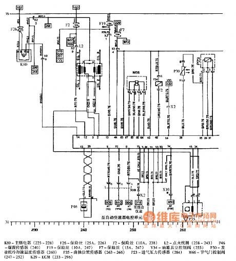
The picture shows the Shanghai GM sail engine circuit.
In the circuit, the K80 is the main relay (225-228). The F126 is fuse (25A, 226). The F2 is fuse (10A, 238). The L2 is ignition coil (238-243). The F46 is knock sensor (240). The F19 is fuse (10A, 247). The F7 is fuse (15A, 247). The Y34 is oil box vacuum control valve (255). The P30is engine cooling fluid temperature sensor (260). The P35 is crankshaft position sensor (263-266). The P23 is intake air pressure sensor (284). The M66 is throttle control valve (247-252). The K29 is ECM (233-296). (View)
View full Circuit Diagram | Comments | Reading(576)
ALTERNATING_RED_GREEN
Published:2009/7/5 23:11:00 Author:May
National LM3909 IC is connected as relaxation oscillator for flashing red and green LEDs alternately. With 12-VDC supply, repetition rate is about 2.5 Hz.Green LED should have its anode or positive lead toward pin 5 as shown for lower LED, where shorter but higher-voltage pulse is available. LED types are not criticaL- Linear Applications, Vol. 2, National Semiconductor, Santa Clara, CA, 1976, AN-154, p 3. (View)
View full Circuit Diagram | Comments | Reading(572)
PHASE_INDICATOR
Published:2009/7/5 23:11:00 Author:May

The circuit provides a simple means of determining the succession of phases of a 3-phase 120 V source used in synchro work. Terminals A, B, and C are connected to the three terminals of the source to be checked. If the neon bulb lights, interchange any two leads; the light then extinguishes and A, B, and C indicate the correct sequence.
If power on any one line is lost, the neon bulb will light. This feature may be useful for monitoring purposes. (View)
View full Circuit Diagram | Comments | Reading(1337)
Floating Signal Source Programmable Gain Amplifier Circuit Composed Of PGA203
Published:2011/7/29 9:10:00 Author:Robert | Keyword: Floating, Signal, Source, Programmable, Gain, Amplifier


The picture shows the floating signal source programmable gain amplifier circuit. This circuit uses digital-control instrumentation amplifier PGA203 integrated chip. Its programmable gain have: 1, 2, 4, 8 (binary). It has low bias current (maximum value is 50pA) and fast setup time (2us can be 0.01%) and low nonlinear distortion (maximum nonlinear distortion is 0.012%) and high CMRR (minimum value is 80dB).
The relations between the control ports A0, A1's voltage level and the gain Av is listed in picture 2. (View)
View full Circuit Diagram | Comments | Reading(573)
SINGLE_FLASH_LED
Published:2009/7/5 23:10:00 Author:May

Mono MVBR connection of National LM3909 IC produces 0.5-s flash with LED each time pushbutton makes momentary contact.- Linear Applications, Vol. 2, National Semiconductor, Santa Clara, CA, 1970, AN-154,p 9.
(View)
View full Circuit Diagram | Comments | Reading(820)
RC_CIRCUIT_DETECTS_PHASE_SEQUENCE_REVERSAL
Published:2009/7/5 23:10:00 Author:May
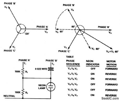
Assume the correct phase sequence to be VA-VB-VC. The circuit terminals are connected such that T1 gets connected to phase A and T2 to phase B. The capacitor advances the voltage developed across R2 due to phase B by - 60°, while the voltages developed across it by phase A is in phase with VA as shown in Fig. 69-1. The net voltage developed across R2~zero, the neon lamp is not energized, thereby signaling correct phase sequence. If terminal T2 gets connected to phase C, a large voltage, K(VA + VC60°), gets developed across R2, energizing the neon indicator to signal reverse phase sequence.
The motor terminals can be connected to the three phases in six different combinations. A three-phase motor will run in the forward direction for three such combinations, while for the other three it will operate in the reverse direction. As shown in the table, the circuit detects all three reverse combinations. This circuit can be wired into any existing motor starter where the operator can see whether the phase sequence has been altered, before starting the machine. (View)
View full Circuit Diagram | Comments | Reading(1605)
05_s_TONE_BURSTS
Published:2009/7/5 23:09:00 Author:May
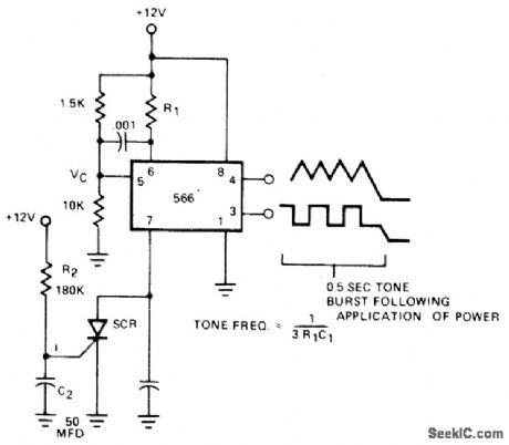
Simple 566 function generator circuit supplies audio tone for 0.5 s after power is applied, for use as communication-network alert signal. SCR is gated on when C2 charges up to its gate voltage, which takes 0.5 s, to shunt timing capacitor between pin 7 and ground and thereby stop tone. If SCR is replaced by NPN transistor, tone can be switched on and off manually at transistor base terminaL- Signetics Analog Data Manual, Signetics, Sunnyvale, CA, 1977, p 852-853. (View)
View full Circuit Diagram | Comments | Reading(710)
SCR_FLASFIES_LED
Published:2009/7/5 23:08:00 Author:May

UJT oscillator Q1 provides timing pulses for triggering SCR driving red Radio Shack 276-041 LED. Circuit draws only 2 mAfrom 9-V battery when producing 12 flashes per second. SCR is 6-A 50-V 276-1089.-F. M. Mims, Semiconductor Proiects, Vol.2, Radio Shack, Fort Worth, TX, 1976, p 78-84. (View)
View full Circuit Diagram | Comments | Reading(914)
| Pages:1072/2234 At 2010611062106310641065106610671068106910701071107210731074107510761077107810791080Under 20 |
Circuit Categories
power supply circuit
Amplifier Circuit
Basic Circuit
LED and Light Circuit
Sensor Circuit
Signal Processing
Electrical Equipment Circuit
Control Circuit
Remote Control Circuit
A/D-D/A Converter Circuit
Audio Circuit
Measuring and Test Circuit
Communication Circuit
Computer-Related Circuit
555 Circuit
Automotive Circuit
Repairing Circuit