
Circuit Diagram
Index 1070
Basic_flash_memory_VSUBPP_SUB_programming_voltage_supply
Published:2009/7/23 22:02:00 Author:Jessie
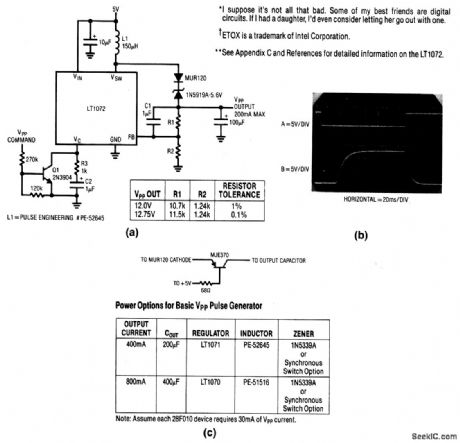
This circuit provides VPP (program power) pulses for programming digital flash memories. Figure 6-48 shows the waveforms involved. Trace A is the programming command. Trace B shows a smoothly rising VPP pulse of the correct amplitude. The amplitude of VPP can be selected by the values of R1 and R2. Figure 6-48C shows a synchronous switch option for the circuit, as well as output currents available with the option. (View)
View full Circuit Diagram | Comments | Reading(700)
Using MAX1298/1299 To Make Up Temperature/Voltage Monitoring System Circuit
Published:2011/8/1 10:52:00 Author:Robert | Keyword: Temperature, Voltage, Monitoring, System

As shown in the picture. This system uses the internal temperature sensor to measure the room temperature. And it uses a 2N3904 type transistor's emitter polar to measure the remote temperature. Other input channels are used to measure the differencial voltage and 0~+5V single-port voltage. The MAX1298/1299 is connected to the uC through the serial interfaces. (View)
View full Circuit Diagram | Comments | Reading(491)
_30V_TO__7V
Published:2009/7/5 23:51:00 Author:May
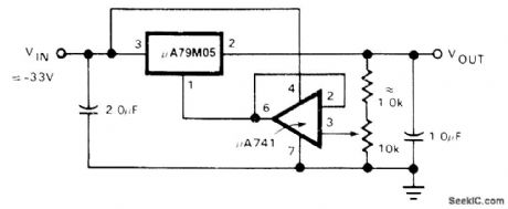
Circuit uses Signetics μA79M05 adjustable voltage regulator in combination with 741 opamp to give wide negative output voltage range. Regulator includes thermal overload protection and internal short-circuit protection. Input voltage should be at least 3V more negative than maximum output volt-age desired.- Signetics Analog Data Manual, Signetics, Sunnyvale, CA, 1977, p 670. (View)
View full Circuit Diagram | Comments | Reading(475)
CONDUCTIVITY_TESTER
Published:2009/7/23 22:01:00 Author:Jessie
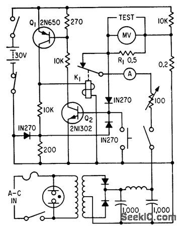
For nondestructive testing of printed-circuit conductors, through hole plating, soldered joints, and coils, in resistance range from 0 to 50 milliohms and currents up to 5 amp. Q1 and Q2 protect millivoltmeter from open-circuit voltage over loads by energizing relay K1, interrupting rectified output from cc power supply.-F. W. Kear, Unit Measures Printed Circuit Resistances, Electronics, 34:4, p 64-65. (View)
View full Circuit Diagram | Comments | Reading(876)
AUDIO_AMPLIFIER
Published:2009/7/5 23:47:00 Author:May

C9 is necessary to filter-out rf input interferences.R3 in combination with C5 is used to limit the af frequency bandwidth.The 470-μF power supply decoupling capacitor is C10. (View)
View full Circuit Diagram | Comments | Reading(1978)
30_KC_HALL_GENERATOR_SAMPLING_SWITCHES
Published:2009/7/23 22:01:00 Author:Jessie
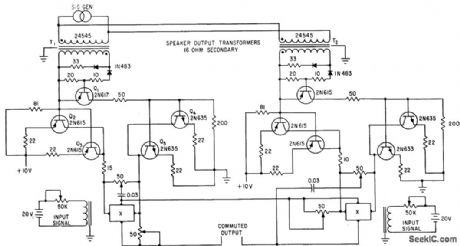
Control current circuits of series-connected Hall generators X are pulsed alternately for switching d-c input signal. Triggering for identical circuit at right occurs on opposite half-cycles of signal generators.-T. J. Marcus, Using Hall Generators as Contactless Commutators, Electronics, 35;4, p 43-45. (View)
View full Circuit Diagram | Comments | Reading(647)
NON_INTEGER_PROGRAMMABLE_PULSE_DIVIDER
Published:2009/7/5 23:46:00 Author:May
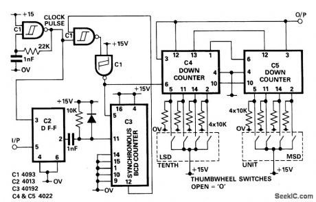
Circuit NotesIn applications where the period of the input pulses is uneven and the divider is required to cover a wide range of frequencies, the non-integer programmable pulse divider shown can be used. The purpose of the D-type flip-flop (IC2) is to synchronize the input signal with the clock pulse. When the clock pulse changes from low to high and the input is high, IC2 output goes high. Subsequently, IC3 resets to zero and starts counting up.The number of pulses at the output of IC3 is ten time the input pulse. IC4 and IC5 are cascaded to form a two decade programmable down counter. (View)
View full Circuit Diagram | Comments | Reading(1007)
KEYBOARD_ENTRY_WITH_4_1_2_DIGIT_DISPLAY
Published:2009/7/5 23:44:00 Author:May

Developed to give keyboard entry of desired frequency for 2-meter frequency as alternative to thumbwhee-switch setting of frequenoy, When key is depressed, mono (one shot) fires, causing CD4022 counter to incre, ment. At same time, keyswitch places appropriate BCD data on input Iines of 74C192 presettable decade counters, Output from counters goes to synthesizer input and to display decoder/driver. LED display may be used in place of LCD display if current drain is not important, Keyboard lockout switch prevents acidental change of gyequency.-M. l. Cohen, A Practical 2m Synthesizer, 73 Magazine, Sept.1977, p n46-151. (View)
View full Circuit Diagram | Comments | Reading(2663)
A Gain-Program-Control Apparatus Amplification Circuit
Published:2011/7/27 3:28:00 Author:Robert | Keyword: Gain, Program, Control, Apparatus, Amplification

The picture shows thea gain-program-control apparatus amplification circuit. (View)
View full Circuit Diagram | Comments | Reading(508)
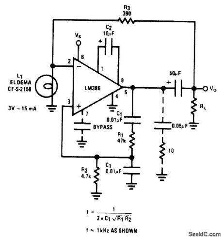
MICRO_SIZED_AMPLIFIER
Published:2009/7/5 23:43:00 Author:May

Sound detected by electret microphone MIC1 is fed to IC1's input through resistor R2, and capacitors C1 and C2. Resistors R2 and R5 determine the overall stage gain, while C2 partially determines the amplifier's frequency response. To ensure proper operation, use a single-ended power supply. R3 and R4 simulate a null condition equal to half the power supply's voltage at IC1's noninverting input. The output of IC1 is transferred to emitter-follower amplifier Q1 via volume control R6. The high-Z-in/low-Z-out characteristic of the emitter-follower matches the moderately high-impedance output of IC1 to a low-impedance headphone load. (View)
View full Circuit Diagram | Comments | Reading(561)
Celsius Temperature And Temperature Difference Measuring Circuit
Published:2011/7/26 21:21:00 Author:Robert | Keyword: Celsius, Temperature, Difference, Measuring

The LM135 series is based on the thermodynamic temperature calibration. If wanting to measure the celsius temperature (t) and celsius temperature difference (△t), it could use the circuits shown in picture (a) and (b). The picture (a)'s circuit's output port is connected to digital voltage meter and it would display the celsius temperature value. The picture (b)'s circuit is used to indicate the temperature difference by using galvanometer. (View)
View full Circuit Diagram | Comments | Reading(680)
PULSE_GENERATOR(ASTABLE_MULTIVIBRATOR)
Published:2009/7/5 23:42:00 Author:May
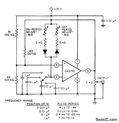
Circuit Notes
Resistors R1 and R2 bias the CA3130 to the mid-point of the supply-voltage, and R3 is the feedback resistor. The pulse repetition rate is selected by positioning S1 to the desired position and the rate remains essentially constant when the resistors which determine on-period and off-period are adjusted. (View)
View full Circuit Diagram | Comments | Reading(980)
1_kHz_WlEN_BRIDGE
Published:2009/7/5 23:40:00 Author:May
Closed-loop gain of 10, fixed by ratio of R1 to R2, is sufficient to avoid spurious oscillations. Frequency is easily changed by using different values for capacitors C1. R3 and lamp L1 provide amplitu e-stabilizing negative feedback. Supply can be 9 V.- Audio Handbook, National Semiconductor. Santa. Clara. CA, 1977. p 4-30-4-33. (View)
View full Circuit Diagram | Comments | Reading(845)
DELAYED_PULSE_GENERATOR
Published:2009/7/5 23:37:00 Author:May
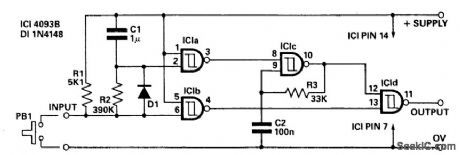
Circuit Notes
The circuit offers independent control of initial delay and pulse rate. IC1c is connected as a pulse generator whose operation is inhibited by the normally low O/P of the IC1a.When the circuit input goes low i.e., by pressing PB1, IC1b O/P goes high and the circuit O/P goes low thus replicating the input. When the input is kept low capacitor C1 charges via R2 to a point where IC1a O/P goes low. This allows the pulse generator IClc to start and rapid fire pulses appear at the circuit O/P. When the circuit input returns to the high state C1 is rapiD1y discharged via D1 and R1. The value of R2 and C1 control the initial delay while R3 and C2 control the pulse rate. The values given will give a delay of around 0.5 seconds and a pulse rate of 200/300 Hz depending on supply voltage. PB1 may be replaced by an open collector TTL gate or a common emitter transistor stage if required. (View)
View full Circuit Diagram | Comments | Reading(0)
200_65000_Hz_WlEN
Published:2009/7/5 23:34:00 Author:May
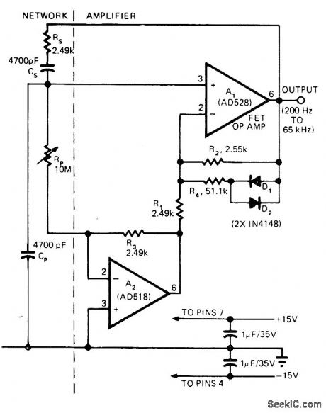
Adding single opamp to Wien-bridge oscillator gives wide-range oscillatorhaving single-control tuning. R4, D1, and D2 together stabilize output amplitude by providing controlled nonlinearity that reduces gain at high signal Ievels. AD528 opamp A1 is FET-input complement to AD518 A2 and has bandwidth required for wide output frequency range.RP sweeps output from 200 Hz to 65 kHz. Since oscillation frequency is inversely proportional to square root of RP, frequency changes rapidly near Iow-resistance end of pot. Use of pot with audio or Iog taper makes tuning more Iinear.-P. Brokaw, FET Op Amp Adds New Twist to an Old Circuit. EDN Magazine. June 5. 1974. p 75-77. (View)
View full Circuit Diagram | Comments | Reading(699)
CHV-CMI48616 Type Induction Cooker Circuit
Published:2011/7/30 19:42:00 Author:Robert | Keyword: Induction Cooker
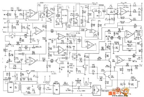
The picture shows the CHV-CMI48616 type induction cooker circuit. (View)
View full Circuit Diagram | Comments | Reading(3064)
55_MHz_presettable_counter
Published:2009/7/5 23:34:00 Author:May

High-speed four-decade counter with preload switches gives positive output pulse 30 ns long at 55 MHz to ensure that all counters are preset to right digit and transients have died out at end of count. If counters are preset to 5555, input fre-quency is counted until countgets to 9997. Next clock pulse triggers auxiliary flip-flop to initiate load pulse (2 cycles long) and get back tozero Total count is 10,000 minus 5555, or 4445 (10-kHz output for 44.5-MHz input.) Article covers construction and testing. Counter draws less than 300 mA at 5 V. Developed for use in 2-meter frequency synthesizer-H. Cross, HighSpeed Divide-by-N Counters, Ham Radio, March 1976, p 36-38. (View)
View full Circuit Diagram | Comments | Reading(1355)
20_dB_AUDIO_ROOSTER
Published:2009/7/5 23:32:00 Author:May

The amphrer's gain is nominally 20 dB.It frequency response is determined primarily by the value of just a few components-primarily C1 and R1.The values in the schematic diagram provide a response of ±3.0 dB from about 120 to over 20,000 Hz. Actually, the frequency response is flat from about 170 to well over 20,000 Hz;it's the low end that deviates from a flat frequency response. The low end's rotloff is primarily a function of capacitor C1, since R1's resistive value is fixed.If C1's value is changed to 0.1μF,the low end's corner frequency-the frequency at which the low end rolloff starts-is reduced to about 70 Hz. If you need an even deeper low end rolloff, change C1 to a 1.0-μF capacitor. If it's an electrolytic type, make certain that it's installed into the circuit with the correct polarity-with the positive terminal con-nected to Q1's base terminal. (View)
View full Circuit Diagram | Comments | Reading(751)
Double_conversion_IF_strip
Published:2009/7/23 22:01:00 Author:Jessie

This circuit shows an SL6700 (Fig. 2-13) connected to form a double-conversion (10.7 MHz and 455 kHz) IF strip, using a ceramic filter for the 455-kHz network. The sensitivity of this circuit is typically 5μV (rms), with 30% modulation for a 10-dB S/N ratio. The circuit will accept up to 100 mV (rms) at 80% modulation with distortion below 5%. (View)
View full Circuit Diagram | Comments | Reading(2217)
AUDIO_CIRCUIT_BRIDGE_LOAD_DRIVE
Published:2009/7/5 23:29:00 Author:May

This circuit shows a method which increases the power capability of a drive system for audio speakers. Two HA-2542s are used to operate on half cycles only, which greatly increases their power handling capability. Bridging the speaker, as shown, makes 200 mA of output current available to drive the load. The HA-5102 is used as an ac-coupled, low noise preamplifier, which drives the bridge circuit. (View)
View full Circuit Diagram | Comments | Reading(743)
| Pages:1070/2234 At 2010611062106310641065106610671068106910701071107210731074107510761077107810791080Under 20 |
Circuit Categories
power supply circuit
Amplifier Circuit
Basic Circuit
LED and Light Circuit
Sensor Circuit
Signal Processing
Electrical Equipment Circuit
Control Circuit
Remote Control Circuit
A/D-D/A Converter Circuit
Audio Circuit
Measuring and Test Circuit
Communication Circuit
Computer-Related Circuit
555 Circuit
Automotive Circuit
Repairing Circuit