
Circuit Diagram
Index 868
FREQUENCY_COUNTER
Published:2009/7/9 22:59:00 Author:May
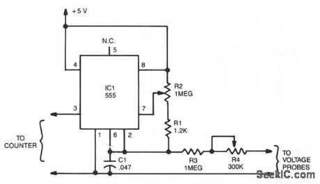
The output frequency from IC pin 3 is determined by the voltage input to pin 6. A standard frequency counter can be used to measure voltages directly over a limited range from 0 to 5 V. In this circuit, the 555 is wired as an astable multi ibrator. Resistor R2 determines the output frequency when the input to the circuit (the voltage measured by the voltage probes) is zero. R4 is a scaling resistor that adjusts the output frequency so that a change in the input voltage of 1 V will result in a change in the output frequency of 10 Hz. That will happen when the combined resistance of R3 and R4 is 1.2 MΩ. To calibrate short the voltage probes together, adjust R2 until the reading on the frequency counter changes to 00 Hz. Then, use the voltage probes to measure an accurate 5-V source and adjust R4 until the frequency counter reads 50 Hz. (View)
View full Circuit Diagram | Comments | Reading(2743)
PLL_TONE_DECODER
Published:2009/7/20 1:52:00 Author:Jessie
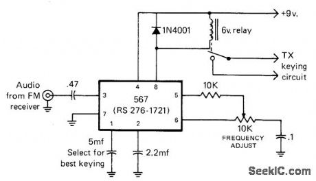
Used in simple wireless FM remote control set up for keying transmit-ter. Keyed 500-Hz tone output of FM receiver at transmitter site acts through 567 PLL to operate 6-V relay whose contacts are in keying circuit of transmitter.-J. Schultz, H.F. Operating-Re mote Control Style, CQ, March 1978, p 22-23 and 90. (View)
View full Circuit Diagram | Comments | Reading(1390)
1_MHz_METER_DRIVER_AMPLIFIER
Published:2009/7/9 22:59:00 Author:May
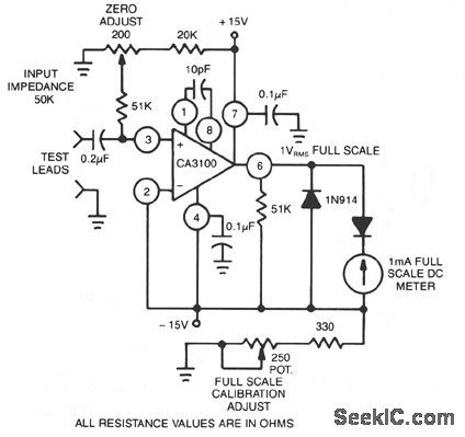
This circuit uses the CA3100 BiMOS op amp to drive a 1-mA meter movement to full scale with 1-V rms input. (View)
View full Circuit Diagram | Comments | Reading(662)
RF_WIDEBAND_ADJUSTABLE_AGC_AMPLIFIER
Published:2009/7/9 22:58:00 Author:May
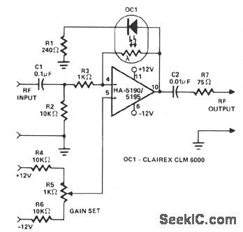
This circuit functions as a wideband adjustable AGC amplifier.With an effective bandwidth of approximately 10 MHz,it is capable of handling rfinput signal frequencies from 3.2 to 10 MHz at levels ranging from 40 mV up to 3 V pk-pk.AGC action is achieved by using optocoupler/isolater OC1 as part of the gain control-feedback loop.In operation, the positive peaks of the amplifed output signal drive the OC1 LED into a conducting state. Since the resistance of the OC1 photosensitive element is inversely proportional to light intensity, the higher the signal level, the lower the feedback resistance to the op amp inverting input. The greater negative feedback lowers stage gain. Any changes in gain occur smoothly because the inherent memory characteristic of the photoresistor acts to integrate the peak signal inputs. In practice, the stage gain is adjusted automatically to where the output signal positive peaks are approximately one diode drop above ground.Gain set control R5 applies a fixed dc bias to the op amp noninverting input, thus establishing the steady state-zero input signal current through the OC1 LED and determining the signal level at which AGC action begins.The effective AGO range depends on a number of factors, including individual device characteristics, the nature of the rf drive signal, the initial setting for R5, et al. Theoretically, the AGC range can be as high as 4000:1 for a perfect op amp because the OC1 photoresistor can vary in value from 1 MΩ with the LED dark to 250 Ω with the LED fully on. (View)
View full Circuit Diagram | Comments | Reading(2474)
ANALOG_VOLTAGE_COMPARATOR
Published:2009/7/20 1:52:00 Author:Jessie
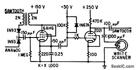
When sawtooth amplitude exceeds analog voltage, positive feedback loop of blocking oscillator is completed through conducting diode and oscillator conducts, triggering thyratron writing circuit for magnetic drum.-H. L. Daniels and D. K. Sampson, Magnetic Drum Provides Analog Time Delay, Electronics, 32:6, p 44-47. (View)
View full Circuit Diagram | Comments | Reading(941)
Z_80_BUS_MONITOR_DEBUGGER
Published:2009/7/9 22:57:00 Author:May
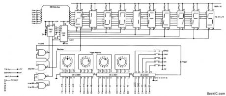
Getting microprocessor designs to work is notoriously difficult when both the software and hardware are new. The usual approach is to run test routines that address memory and I/0, but do not rely on their correct functioning. However, miswiring in any part of the circuit usually leads to a misleading jumble of signals that might require a logic analyzer to interpret.
This simple circuit will trace the program execution and help point to the problems. Although the circuit shows connections for a Z-80, the circuit can very easily be adapted for any 8-bit microprocessor or with additional circuitry for CPUs of any bus width.
The circuit consists of a 5-byte hexadecimal display and comparator, which are wired to a 40-pin IC test clip. The test clip sits over the microprocessor (in this case a Z-80), where it gets power and all the required signals. The address bus and control lines are fed to the comparator, where (by means of switches) a trigger condition can be set. Following the trigger, the next 5 occurrences of either RD or WR will latch the contents of the data bus into the 5 hex displays, each in turn.
For example, select address 0000 M1 Rd and reset the CPU. The displays will show the very first instruction fetch, followed by its data and any consequent action. Even details, such as stack writes and subroutine addresses, are included. lb trace longer por-tions of a program the address switches can be incremented to follow the execution path. (View)
View full Circuit Diagram | Comments | Reading(724)
BLIP_AND_HOLD_RADIO_CONTROL
Published:2009/7/20 1:50:00 Author:Jessie
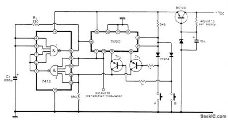
Coder uses two ICs to generate sequence of pulses suitable for actuators of radio control system. During standby, oscillator formed by NAND gate 1 operates at 0.5 Hz as determined by C1 and R1, and all four outputs of 7490 IC are zero. When switch AL is closed, 7490 is clocked by negative edge of oscillator waveform and Tr1 becomes forward-biased. Output of NAND gate 2 then drops to zero, stopping oscillator and holding outputs of 7490. When switch A is opened, outputs of 7490 again drop to zero. Many different blip-and-hold combinations can be obtained by suitable arrangement of switches and gates.-G. D. Southern, Sequence Generator for Radio Control, Wireless World, Jan. 1976, p 60. (View)
View full Circuit Diagram | Comments | Reading(838)
LIGHTS_ON_SENSOR
Published:2009/7/9 22:56:00 Author:May
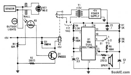
Remote monitoring of a light source is possible with this circuit.Photocell R3 activates Q1 and relay K1. U1 is a tone generator that drives a small speaker. (View)
View full Circuit Diagram | Comments | Reading(1090)
DATA_LINE_REMOTE_SHORT_SENSOR
Published:2009/7/9 22:54:00 Author:May
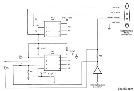
Sensing short circuits in equipment that performs under water is especially critical, but Fig. 20-4's wet-mate connector design also suits other remote short-circuit sensing applications. Because of the limits imposed by the battery and voltage levels, the circuit uses the data line to sense short circuits.
The differential voltage that develops across the 422-Ω resistor in the data line drives a low-bandwidth op amp, which amplifies and filters the differential signal. The resistor values produce a gain of 3. The op amp's output controls the voltage regulator's shutdown pin.
To operate correctly, the circuit must have a continuous stream of digital data. Under normal conditions, and using high-speed CMOS logic, the data source sinks less than 10 μA. This normal operation generates about -3 mV across the sense resistor. The op amp's output will be slightly negative, producing a solid ON signal to the voltage-regulator chip. When a short occurs, the resistor and op amp together produce an average of 2.4 Vdc. This voltage provides a solid OFF to the voltage-regulator chip.
The peak signal-line current is about 12 mA (5-V data divided by 422 Ω), which HCMOS logic can handle. The addition of the resistor and op amp only changes the rise time to about 40 ns and doesn't cause any problems with the 2.5-MHz data rate. When the short is no longer present, the voltage regulator chip turns on again. You can use the same circuit with any TTL on/off-type voltage-regulator IC. (View)
View full Circuit Diagram | Comments | Reading(1098)
BEEPER_FOR_TELEPHONE_RECORDING
Published:2009/7/20 1:49:00 Author:Jessie
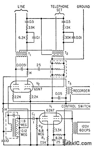
Generates periodic 1,400-cps tone or beep having 0.2 sec duration, at intervals of about 15 sec, as required by Federal law when recording or broadcasting telephone conversations.-J. Zelle, Phone Calls for Broad-cast, Electronics, 31:45, p 96-101. (View)
View full Circuit Diagram | Comments | Reading(655)
AUTOMATIC_EMERGENCY_LIGHTING_UNIT
Published:2009/7/9 22:53:00 Author:May
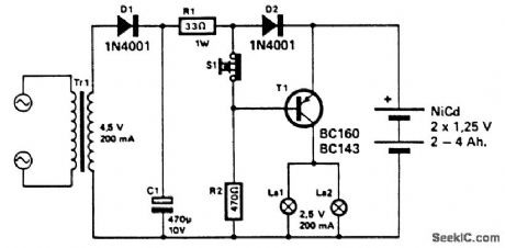
This unit uses a Nicad battery to provide power to an emergency lighting setup. When power fails, T1 becomes forward biased, which lights L1 and L2. The batteries are normally kept charged. When power is on, T1 is cut off and it keeps the lamps extinguished. (View)
View full Circuit Diagram | Comments | Reading(990)
450_MHz_COMMON_GATE_AMPLIFIER
Published:2009/7/9 22:52:00 Author:May
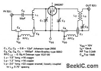
This is a low nolse,3-dB typical NF,amplifier with about 10-dB gain at 450-470 MHz for VHF two-way applications. (View)
View full Circuit Diagram | Comments | Reading(625)
WIRELESS_REMOTE_TU_NING
Published:2009/7/20 1:49:00 Author:Jessie
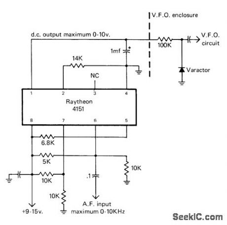
Frequency-to-voltage converter for transceiver responds to AF output of control receiver and feeds corresponding DC voltage to varactor tuning diode in VFO of transceiver, for remote wireless tuning. In most cases only a few volts of DC variation across varactor are sufficient, so variable audio oscillator at remote-control location need have range of only a few kilohertz.-J. Schultz, H.F. Operating-Remote Control Style, CQ, March 1978, p 22-23 and 90. (View)
View full Circuit Diagram | Comments | Reading(620)
3_μP_I_O_LINE_PROTECTORS
Published:2009/7/9 22:51:00 Author:May
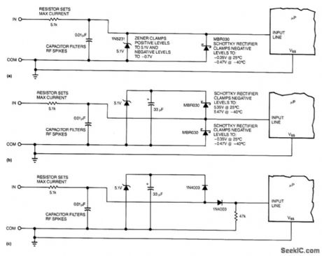
In Fig. 20-3(a), a 5.1-V zener diode clamps positive-going transients, and a Schottky rectifier clamps negative-going transients. The Schottky rectifier has problems at both ends or the temperature scale. At 125℃ (2570F), its leakage current can reach 50 μA when the input line is at 5 V. This leakage is not a big deal unless the input resistor has a value of 100 kΩ or more. More troubling, at temperatures below -40℃ (-400F), the Schottky rectifier's forward voltage rises to about 0.47 V, which is perilously close to the -0.50 -V max spec that most HCMOS-type μPs inputs can tolerate.
The third circuit, Fig. 20-3(c), uses two regular silicon rectifiers. One rectifier is connected in series with the input line, thereby isolating the μPs inputs from negative-going voltage spikes. The other recti-fter is in series with a 5.1-V zener, which clamps positive-going transients. (View)
View full Circuit Diagram | Comments | Reading(836)
LIGHT_DIMMER
Published:2009/7/9 22:51:00 Author:May
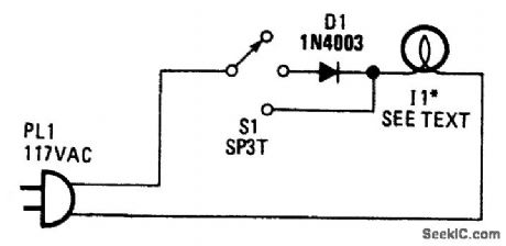
Lamp I1 is a household lamp. When the switch is in the center position, the lamp is operated on half-wave rectified ac; the effective voltage the lamp sees is less, which dims it. I1 can be a lamp up to 200 W or 50 rated at 120 or 240 V, and D1 should be a 200-V PlV or better diode (400PIV for 240-V operation). (View)
View full Circuit Diagram | Comments | Reading(675)
HIGH_NPUT_RESISTANCE_VOLTMETER
Published:2009/7/9 22:51:00 Author:May
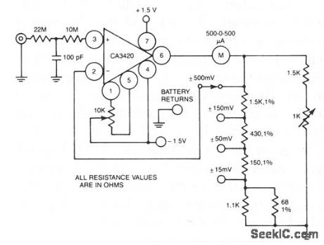
A resistance of 1,000,000 MΩ takes advantage of the high input impedance of the CA3420 BiMOS op amp. Only two 1.5-V AA-type penlite batteries are required for use. Full-scale deflection is ±1500 mV. ±150 mV and ±15 mV. (View)
View full Circuit Diagram | Comments | Reading(808)
2_30_MHz_AMPLIFIER
Published:2009/7/9 22:51:00 Author:May
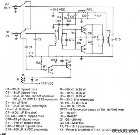
This amplifier provides 140-W PEP nominal output power when supplied with input levels as low as 3 W. Both input and output transformers have a 4:1 turn ratio and a 16:1 impedance ratio to achieve low input VSWR across the band with high-saturation capability. (View)
View full Circuit Diagram | Comments | Reading(756)
10_dB_GAIN_AMPLIFIER
Published:2009/7/9 22:50:00 Author:May
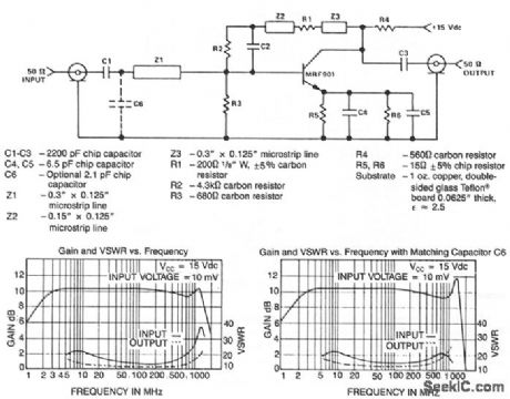
This circuit design is a class A amplifier employing both ac and dc feedback. Bias is stabilized at 15 mA of the collector current using dc feedback from the collector. The ac feedback, from collector to base, and in each of the partially bypassed emitter circuits, compensates for the increase in device gain with decreasing frequency, yielding a flat response over a maximum bandwidth. The amplifter shows a nominal 10-dB power gain from 3 MHz to 1.4 GHz. With only a minimum matching network used at the amplifier input, the input VSWR remains less than 2.5:1 to approximately 1 GHz, while the output VSWR stays under 2:1. Note that a slight degradation in gain flatness and output VSWR occurs with the addition of C6. A more elaborate network design would probably optimize impedance matching, while maintaining gain flatness. (View)
View full Circuit Diagram | Comments | Reading(1275)
1296_MHz_SOLID_STATE_POWER_AMPLIFIER
Published:2009/7/9 22:48:00 Author:May
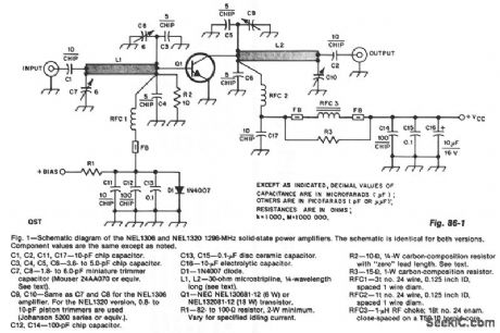
The design incorporates 30-Ω,1/4λmicrostrip lines on the input and output.C3,C4,C7,and C8,along with L1, from a pi network that matches the low-input impedance ofthe device to 50 Ω.C5,C6,C9,C10,and 30-Ω transmission line L2 form an outputpl network that maxlmlzes power transfer to 50 Ω.C10 is not always necessary, depending on variations among devices and circuitboard material.Bias is provided by R1,R2,and D1.R1 can be optimized, if desired,to adjust the collector idling current. (View)
View full Circuit Diagram | Comments | Reading(1528)
HIGH_IMPEDANCE_DIFFERENTIAL_INPUT
Published:2009/7/9 22:48:00 Author:May
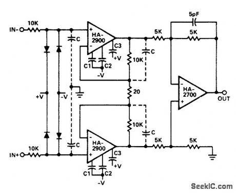
Two Harris HA-2900 chopper-stabilized opamps feed HA-2700 high-performance opamp for instrumentation applications. Circuit provides excellent rejection of ±10 V common-mode input signals. Protection diodes prevent voltages at input terminals from exceeding either power supply. Supply can be ±15 V.- Linear & Data Acquisition Products, Harris Semiconductor, Melbourne, FL, Vol. 1, 1977, p 7-70 (Application Note518). (View)
View full Circuit Diagram | Comments | Reading(780)
| Pages:868/2234 At 20861862863864865866867868869870871872873874875876877878879880Under 20 |
Circuit Categories
power supply circuit
Amplifier Circuit
Basic Circuit
LED and Light Circuit
Sensor Circuit
Signal Processing
Electrical Equipment Circuit
Control Circuit
Remote Control Circuit
A/D-D/A Converter Circuit
Audio Circuit
Measuring and Test Circuit
Communication Circuit
Computer-Related Circuit
555 Circuit
Automotive Circuit
Repairing Circuit