
Circuit Diagram
Index 880
NICAD_BATTERY_TESTER
Published:2009/7/9 21:08:00 Author:May
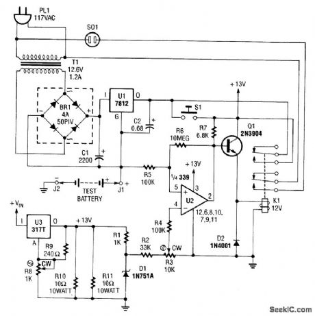
This Nicad battery tester discharges the test battery at a rate of 500 mA.When the endpoint of 1 V(determined by setting of R3) is resolved,pin 2 of U2 becomes low, deactivating Q1 and disconnecting thetest battery from the circuit, Power for U3 comes from the 12-V regulator h series with the battery beingtested, A clock or timer can be plugged into S1 to indicate the time it takes to discharge the battery undertest. (View)
View full Circuit Diagram | Comments | Reading(905)
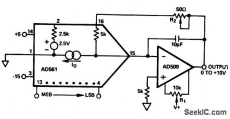
10_bit_D_A_converter_connected_for_four_quadrant_multiplication_
Published:2009/7/20 4:17:00 Author:Jessie
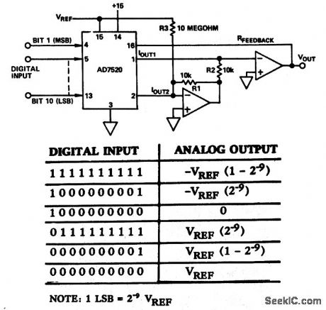
10-bit D/A converter connected for four-quadrant multiplication (courtesy Analog Devices, Inc.). (View)
View full Circuit Diagram | Comments | Reading(772)
PROGRAMMABLE_GAIN_DIFFERENTIAL_INPUT_AMPLIFIER
Published:2009/7/9 21:08:00 Author:May
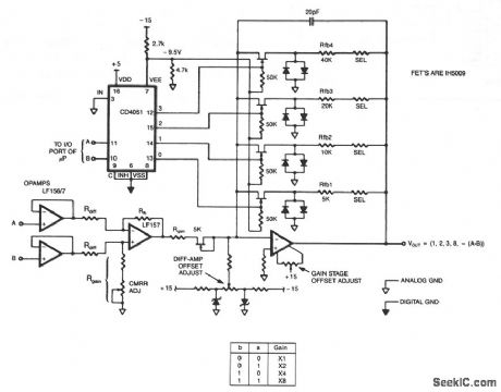
This programmable gain circuit employs a CD4051 CMOS Analog Multiplexer as a two to four line decoder, with appropriate FET drive for switching between feedback resistors to program the gain to any one of four values. (View)
View full Circuit Diagram | Comments | Reading(2689)
5_AMP_AT_0_TO_20_V
Published:2009/7/20 4:16:00 Author:Jessie
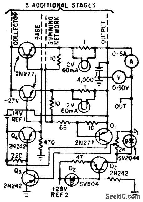
Five regulator transistors in 5-amp power supply have indicator lamps at their emitters. Regulation is better than 0.1% at 20 v, and ripple is below 1 my rms.-J. A. Wheeler and E. J. Currence, Faull-Indicating Series Regulator, Electronics, 34:4, p 60. (View)
View full Circuit Diagram | Comments | Reading(540)
SMALL_CURRENT_AMPLIFIER
Published:2009/7/9 21:08:00 Author:May
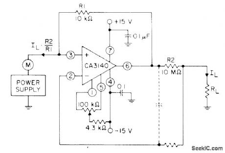
CA3140 bipolar MOS opamp serves as high-gain current amplifier. Input current through load is increased by ratio of R2 to R1, which is 1000 for values shown, for reading by meter M. Dashed lines show method of decoupling circuit from effects of high output-lead capacitance.- Circuit Ideas for RCA Linear ICs, RCA Solid State Division, Somerville, NJ, 1977, p 13. (View)
View full Circuit Diagram | Comments | Reading(801)
12_bit_successive_approximation_A_D_converter_for_unipolar_0_to__10_volt_input_range_with_buffer_follower
Published:2009/7/20 4:16:00 Author:Jessie
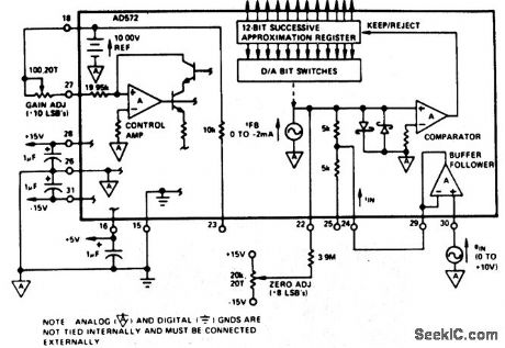
12-bit successive approximation A/D converter for unipolar 0 to +10-volt input range with buffer follower. A/D chip is the AD572 (courtesy Analog Devices, Inc.). (View)
View full Circuit Diagram | Comments | Reading(854)
DIGITALLY_PROGRAMMABLE_PRECISION_AMPLIFIER
Published:2009/7/9 21:06:00 Author:May
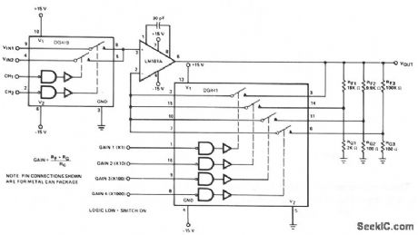
The DG419 looks into the high input impedance of the op amp, so the effects of RDS(on) are negligible.The DG441 is also connected in series with RIN and is not included in the feedback dividers, thus contributing negligible error to the overall gain. Because the DG419 and DG441 can handle ±15 V, the unity gain follower connection, X1, is capable of the full op-amp output range of ±12 V. (View)
View full Circuit Diagram | Comments | Reading(770)
DUAL_TRACE_CONVERTER
Published:2009/7/20 4:15:00 Author:Jessie
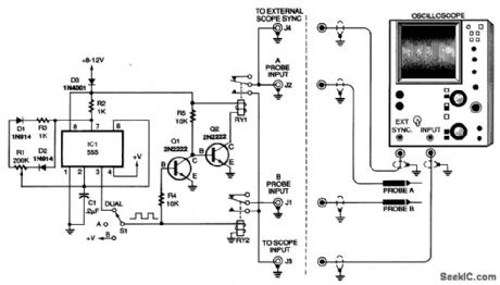
The probe switching circuit is shown in the figure. Two SPST reed relays, RY1 and RY2, switch the signal from two probes to a single scope input. Reed relays provide smooth and noise-free switching. The input side of each relay is connected to a scope probe, and the outputs of the relays are tied together and connected to the scope's single-channel input. A 555 timer, IC1, is con-figured as a variable-duty-cycle square-wave oscillator. Potentiometer R1 varies the oscillator's duty cycle to compensate for response-time variations that different relays might have. The potentiometer is adjusted to give equal brightness to both of the signals being displayed on the oscilloscope. If the relays you choose work well with a 50-percent duty cycle, the potentiometer can be replaced with two fixed resistors wired in series, with the junction between the two resistors connected to pin 2 of IC1. With the parts values shown, the timer has an output frequency of about 80 Hz. Switch S1 allows independent viewing of each oscilloscope trace. When S1 connects pin 3 of IC1 to the coil of RY2 and R4, both input traces will be displayed. When S1 connects +V to the coil of RY2 and R4, only channel B will be displayed. With the switch in the center OFF position, only the channel-A signal is displayed. (View)
View full Circuit Diagram | Comments | Reading(980)
VOLTAGE_TO-FREQUENCY_CONVERTER_1
Published:2009/7/9 21:04:00 Author:May
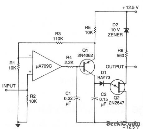
This circuit consists of a UJT oscillator in which the timing charge capacitor C2 is linearly dependent on the input signal voltage. The charging current is set by the voltage across resistor R5, which is accurately controlled by the amplifier. (View)
View full Circuit Diagram | Comments | Reading(558)
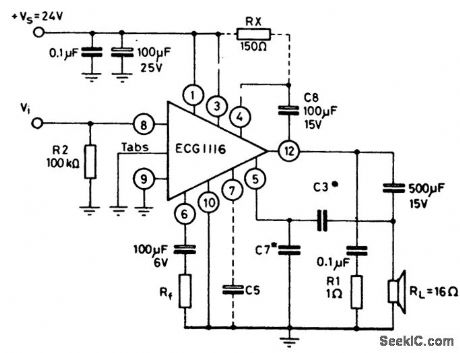
5_watt_AF_power_amplifier_with_16_ohm_load_connected_to_ground_using_no_bootstrap
Published:2009/7/20 4:15:00 Author:Jessie
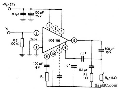
5-watt AF power amplifier with 16-ohm load connected to ground using no bootstrap. The ECG1116 is a 12-pin QIP. To obtain the rated output heatsinking is required. Capacitor C3 is typically 330 pF, while C7 is 1500 pF. Generally C7 is five times greater than C3. Supply voltage ripple rejection is improved by connecting a capacitor (10 to 100 μF at 25 volts) between pin 7 and ground. Frequency response is from 40 hertz to 20 kilohertz (courtesy GTE Sylvania Incorporated). (View)
View full Circuit Diagram | Comments | Reading(792)
VOLICE_MODULATED_PULSE_FM_IR_TRANSMITTER
Published:2009/7/9 21:04:00 Author:May
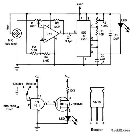
This circuit has a 741 audio amplifier, which is fed by a microphone (use an amplified type), an FM modulator, and a CMOS timer that acts as a VCO. The LED is pulsed with the timer output (the booster circuit can be used for increased range). This yields an FM-modulated, pulsed IR beam. (View)
View full Circuit Diagram | Comments | Reading(2515)
V_F_converter_with_20_kHz_full_scale_output
Published:2009/7/20 4:15:00 Author:Jessie
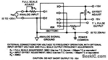
V/F converter with 20 kHz full scale output (courtesy Analog Devices, Inc.). (View)
View full Circuit Diagram | Comments | Reading(857)
5_watt_AF_power_amplifier_with_16_ohm_load_connected_to_ground_and_using_bootstrap
Published:2009/7/20 4:14:00 Author:Jessie

5-watt AF power amplifier with 16-ohm load connected to ground and using bootstrap. For low voltage operation (e.g., 9 to 14volts) 150 ohms is connected between pins 1 and 4. To improve power supply ripple rejection capacitor C5 (10 to 100 μF at 25 volts) is connected between pin 7 and ground. Capacitor C3 is typically 330 pF and C7 is 1500 pF. Generally C7 is five times greater than C3 Frequency response is from 40 hertz to 20 kilohertz (courtesy GTE Sylvania Incorporated). (View)
View full Circuit Diagram | Comments | Reading(553)
BATTERY_TESTER
Published:2009/7/9 21:03:00 Author:May
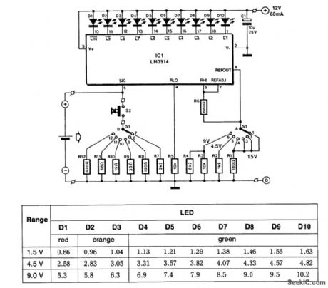
This battery tester makes use of an LM3914 bar-graph driver IC. S1 selects load on battery under test and programs the voltage range. S2 loads the battery under test. The table gives the calibration factors for the tester. LEDs D1 through D10 are used as indicators. (View)
View full Circuit Diagram | Comments | Reading(4275)
A_D_converter_with_sample_and_hold_circuit_for_bipolar_operation±5_volts
Published:2009/7/20 4:14:00 Author:Jessie
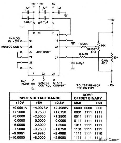
A/D converter with sample-and-hold circuit for bipolar operation,±5 volts. For ±2.5-volt operation jumper pins 22 and 25 with the connections shown. For ±10-volt operation change the jumper at pin 29 from pin 24 to pin 25 and leave all otters as shown (courtesy Datel Systems, Inc.). (View)
View full Circuit Diagram | Comments | Reading(847)
10_bit_and_sign_multiplying_D_A_converter_
Published:2009/7/20 4:13:00 Author:Jessie
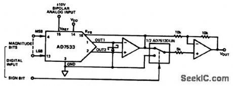
10-bit and sign multiplying D/A converter (courtesy Analog Devices, Inc.). (View)
View full Circuit Diagram | Comments | Reading(757)
NONLATCHING_RELAY
Published:2009/7/9 21:03:00 Author:May
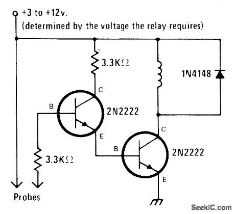
When liquid rises above level determined by positions of probes, circuit is triggered and relay, buzzer, or other indicator is energized. Alarm stops when liquid drops below preset level again. Use any operating voltage from 3 to 12 V that will actuate load employed.-J. A. Sandier, 9 Easy to Build Projects under $9, Modern Electronics, July 1978, p 53-56. (View)
View full Circuit Diagram | Comments | Reading(1055)
10_bit_D_A_converter_with_0_to__10_volt_unipolar_output
Published:2009/7/20 4:12:00 Author:Jessie
10-bit D/A converter with 0 to +10-volt unipolar output (courtesy Analog Devices, Inc.). (View)
View full Circuit Diagram | Comments | Reading(780)
WIDE_RANGE_DIGITALLY_CONTROLLED_VARIABLE_GAIN_AMPLIFIER
Published:2009/7/9 21:02:00 Author:May
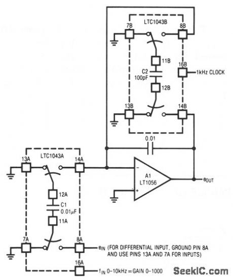
The circuit uses the LTC1043 in a variable gam amplifier which features continuously variable gain, gain stability of 20 ppm/℃, and single-ended or differential inputs. The circuit uses two separate LTC1043s. LTC1043B is continuously clocked by a 1-kHz source, which could also be processor supplied. Both LTC1043s function as the sampled data equivalent of a resistor within the bandwidth set by A1's 0.01-μF value and the switched-capacitor equivalent feedback resistor. The time-averaged current delivered to the summing point by LTC-1043A is a function of the 0.01-μF capacitor's input-derived voltage and the commutation frequency at pin 16. Low-commutation frequencies result in small time-averaged current values, and require a large input resistor. Higher frequencies require an equivalent small input resistor. (View)
View full Circuit Diagram | Comments | Reading(669)
INFRARED_REMOTE_CONTROL_TESTER
Published:2009/7/9 21:02:00 Author:May
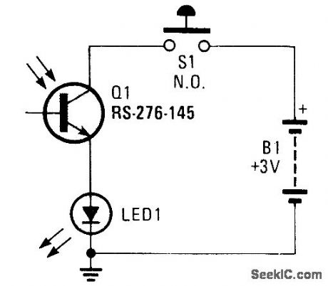
Using a battery, a phototransistor and a visible-light LED, this simple circuit is a go/no go tester for IR remote control devices. The illumination of the LED indicates that Q1 is being modulated by IR energy. (View)
View full Circuit Diagram | Comments | Reading(0)
| Pages:880/2234 At 20861862863864865866867868869870871872873874875876877878879880Under 20 |
Circuit Categories
power supply circuit
Amplifier Circuit
Basic Circuit
LED and Light Circuit
Sensor Circuit
Signal Processing
Electrical Equipment Circuit
Control Circuit
Remote Control Circuit
A/D-D/A Converter Circuit
Audio Circuit
Measuring and Test Circuit
Communication Circuit
Computer-Related Circuit
555 Circuit
Automotive Circuit
Repairing Circuit