
Circuit Diagram
Index 877
VOLTAGE_CURSOR_ADAPTER
Published:2009/7/20 4:08:00 Author:Jessie
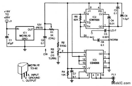
This is the schematic diagram for the voltage cursor adapter. The required 15- to 25-V power to the circuit can be supplied either by batteries or by a wall-mounted ac to 15-Vdc adapter. The MC78L12 voltage regulator (IC1) supplies regulated 12 Vdc to the rest of the circuit. The ICM7555 timer (IC2) drives the CD4066B, a CMOS bilateral switch (IC3). This drive frequency can either be a normal frequency (NORM) of 100 kHz or a low frequency (LO-F) of 10 kHz, depending on the setting of switch S1. Set S1 to LO-F for inputs below 500 Hz. The dc reference voltage supplied to pin 3 of IC3 is set by R3, a 10-turn, 5000-Ω precision potentiometer. The voltage can be read directly from a turns counter dial coupled directly to the potentiometer's wiper. The accuracy of this reading can be 1 per-cent or better. Trimmer potentiometer R1 permits the voltage to R3 to be calibrated to precisely 10 V. The circuit is calibrated by setting the digital reading on the turns counter of R3 to the full clockwise position and adjusting R1 for a reading of 10 V at the wiper of R3 with a digital voltmeter. Bilateral switch IC3 converts the dc reference to a square wave with exactly the same wiper amplitude. The square-wave output appears on the common pins 4, 9, and 10 of IC3 aqd coaxial plug PL1. (View)
View full Circuit Diagram | Comments | Reading(1117)
HOME_SECURITY_SYSTEM
Published:2009/7/9 21:45:00 Author:May
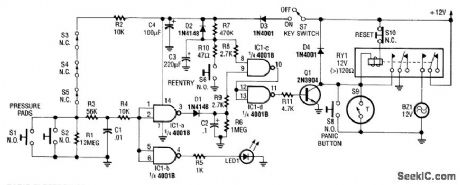
This alarm circuit activates when S1 through S5 are activated. This lights LED1 and activates Q1 via IC1C and IC1D. RY1 is wired to self latch. S10 is used to reset. When key switch S1 is activated or when re-entry buttons at S6 are depressed, IC1C is deactivated until RC network R7/C3 charges. (View)
View full Circuit Diagram | Comments | Reading(1689)
10_bit_D_A_converter_with_±10_volt_buffered_output
Published:2009/7/20 4:08:00 Author:Jessie
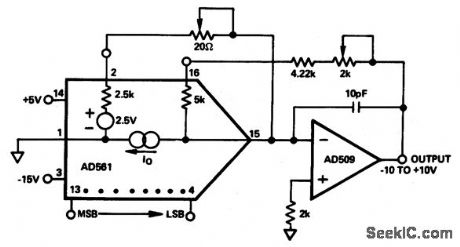
10-bit D/A converter with ±10-volt buffered output (courtesy Analog Devices, Inc.) (View)
View full Circuit Diagram | Comments | Reading(776)
VERY_LOW_DUTY_CYCLE_PULSE_GENERATOR
Published:2009/7/9 21:45:00 Author:May
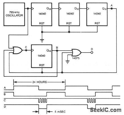
Using a precision oscillator and a few CMOS counters, you can build a precise, very low duty-cycle pulse generator. You can add as many counters as you desire to make the period as long as you wish. The circuit will generate a pulse about 5 ms long every 24 hours-one 5.9 -6% duty cycle (View)
View full Circuit Diagram | Comments | Reading(704)
300_V_PULSE_GENERATOR
Published:2009/7/9 21:44:00 Author:May
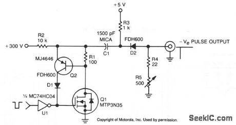
In this TMOS pulser, a negative-going pulse is applied to U1, a high-speed CMOS buffer, which directly drives the gate of Q1, an MTP3N35. If only a 100-V pulse is required, the MTA6N10 can be used.The pulse output across R2 is differentiated by R3/C1 and appears as a negative-going spike at the output terminal. (View)
View full Circuit Diagram | Comments | Reading(556)
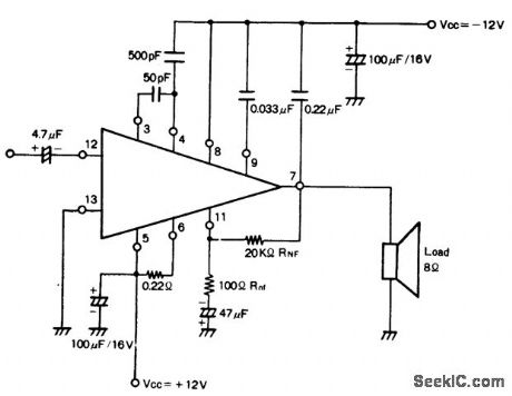
20_watt_single_ended_AF_power_amplifier
Published:2009/7/20 4:08:00 Author:Jessie
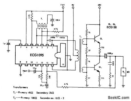
20-watt single-ended AF power amplifier. The ECG1095 is a 14-pin DIP with a tab and built-in AGC. The two output transistors are ECG130 bipolars (courtesy GTE Sylvania Incorporated). (View)
View full Circuit Diagram | Comments | Reading(620)
Power_D_A_converter_using_the_AD7520
Published:2009/7/20 4:07:00 Author:Jessie
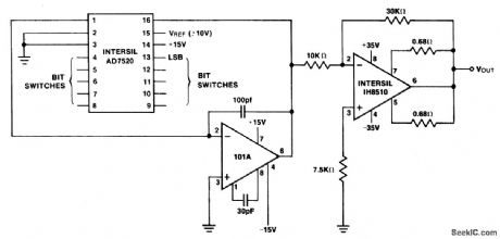
Power D/A converter using the AD7520.The Intersil AD7520 is an 18-pin multiplying DIA converter. This circuit is designed for 8-bit accuracy and 10-bit resolution.The Intersil IH8510 power amplifier(1A continuous output) is driven by the AD7520.A summing amplifier between the AD7520 and IH8510 is used to separate the gain block containing the AD7520 on-chip resistors from the power amplifier stage,whose gain is set only by the external resistors.This approach minimizes drift, otherwise the AD7520 can be directly connected to the IH8510 by using a 25-volt reference for the D/A converter(courtesy Intersil, Inc.). (View)
View full Circuit Diagram | Comments | Reading(1795)
LOGIC_PULSER
Published:2009/7/9 21:42:00 Author:May
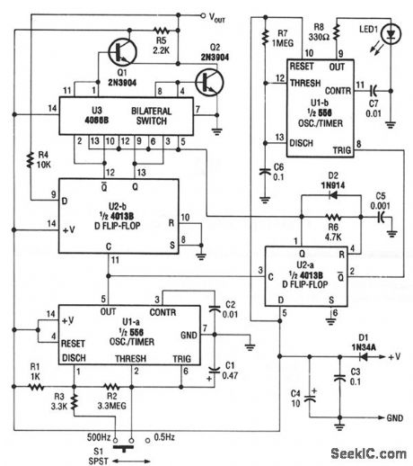
The pulser generates pulses at a user-selected frequency of 0.5 or 500 Hz, with a pulse width of about 5 ms. If the input to be pulsed is already being driven high or low by another output, the pulser automatically pulses the input to the opposite logic state. The pulser is powered by the circuit under test, and operates from supplies of from + 5 to + 15 Vdc. (View)
View full Circuit Diagram | Comments | Reading(1937)
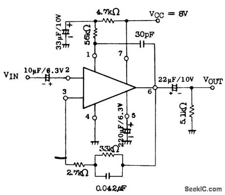
LOW_DRIFT_LOW_NOISE_dc_AMPLIFIER
Published:2009/7/9 21:42:00 Author:May
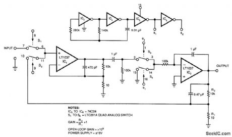
Figure 39-2's circuit combines a low-noise op amp, IC1, with a chopper-based carrier-modulation scheme to achieve a low-noise, low-drift dc amplifier whose performance exceeds any currently available monolithic amplifier. The amplifier's offset is less than 1μV/℃, and its drift is less than 0.05 μV. This circuit has noise within a 10-Hz bandwidth less than 40 nV. The amplifier's bias current, which is set by the bipolar input of IC1, is about 25 nA.
The 74C04 inverters (IC3 to IC6) form a simple 2-phase square-wave clock that runs at about 350 Hz.The complementary oscillator signals (Q1 and Q2) provide drive to S1 and S2,respectively, causing a chopped version of the input to appear at 101's input. IC1 amplifies this ac signal. S3 and S4 synchronously demodulate 101's square-wave output. Because 53 and 54 switch synchronously with S1 and S2, the cir-cuit presents proper amplitude and polarity information to IC2, the dc output amplifier. This output stage integrates the square wave to provide a dc voltage output. R1 and R2 divide the output and feed it back to the input chopper where the divided output serves as a zero signal reference. The ratio of RI and R2 sets the gain, in this case to 1000. (View)
View full Circuit Diagram | Comments | Reading(675)
65_watt_AF_power_amplifier_using_an_ECG1078_chip_powered_by_a_single_24_volt_supply
Published:2009/7/20 4:06:00 Author:Jessie
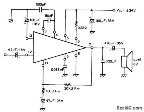
6.5-watt AF power amplifier using an ECG1078 chip powered by a single 24-volt supply. Frequency response is from 100 hertz to 20 kilohertz (courtesy GTE Sylvania Incorporated). (View)
View full Circuit Diagram | Comments | Reading(610)
SIMPLE_BURGLAR_ALARM_1
Published:2009/7/9 21:41:00 Author:May
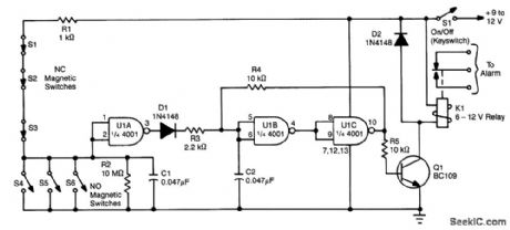
Using one IC and a driver transistor, this simple alarm uses either NO or NC sensors,When a sensoroperates,the input to U1A goes low,causmg U1A to go high,U1B low,and U1C high.This biases Q1 ONand activates relay K1.On/offis vla keyswitch S1. (View)
View full Circuit Diagram | Comments | Reading(691)
PROXIMITY_SENSOR
Published:2009/7/9 21:40:00 Author:May
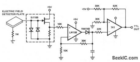
The Si1100 series circuit input is connected to a capacitive field sensor-possibly a piece of doublesided circuit board. Any induced voltage change on the plate is fed to the input of the peak detector section of the op-amp circuit. The Schmitt trigger monitors the voltage across the capacitor and changes its output state when the capacitor voltage crossed the 2.5-trigger point. The output from the Schmitt trigger switches between 0 and 5 V and is microprocessor compatible for sensor applications, such as computer-controlled intruder alarms. (View)
View full Circuit Diagram | Comments | Reading(2320)
65_watt_AF_power_amplifier_using_an_ECG1078_chip_powered_by_±12_volt_supplies
Published:2009/7/20 4:28:00 Author:Jessie
6.5-watt AF power amplifier using an ECG1078 chip powered by ±12-volt supplies. Frequency response is from 100 hertz to 20 kilohertz (courtesy GTE Sylvania Incorporated). (View)
View full Circuit Diagram | Comments | Reading(885)
SIMPLE_BURGLAR_ALARM
Published:2009/7/9 21:39:00 Author:May
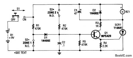
A simple circuit using either NO or NC sensors uses an RC delay circuit (R2/C2 or R1/C2) to drive emitter-follower Q1, switching SCR1 and buzzer (or bell) BZ1. S1 is used for activation and reset. (View)
View full Circuit Diagram | Comments | Reading(765)
10_bit_DIA_converter_with_an_AD509_op_amp
Published:2009/7/20 4:27:00 Author:Jessie
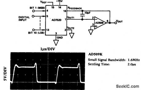
10-bit DIA converter with an AD509 op amp(courtesy Analog Devices, Inc.). (View)
View full Circuit Diagram | Comments | Reading(843)
Equalizer_amplifier_for_cassette_tape_recorders_using_an_ECG1087_module
Published:2009/7/20 4:27:00 Author:Jessie
Equalizer amplifier for cassette tape recorders using an ECG1087 module. Typical voltage gain is 35 dB (courtesy GTE Sylvania Incorporated). (View)
View full Circuit Diagram | Comments | Reading(475)
SCR_PROXIMITY_ALARM
Published:2009/7/9 21:38:00 Author:May
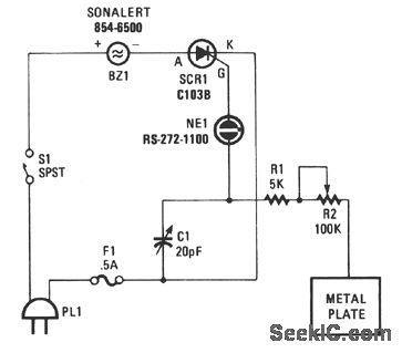
View full Circuit Diagram | Comments | Reading(646)
VOLTAGE_CONTROLLED_PHASE_SHIFT_OSCILLATOR
Published:2009/7/20 4:27:00 Author:Jessie
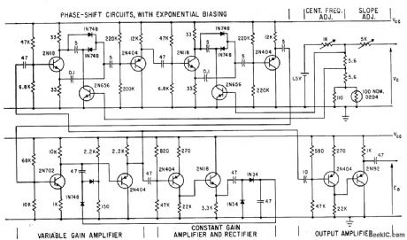
Small-signal a-c resistance of junction diode, related to reciprocal of junction current over two-decade range, is used in two-section R-C phase-shift network acting with amplifier and agc to give constant-amplitude voltage-controlled oscillator with frequency range of over two decades.-R. A. Greiner and S. K. Morgan, Voltage Controlled Wide-Range Oscillator, Electronics, 34:51, p 31-35. (View)
View full Circuit Diagram | Comments | Reading(1376)
400_Hz_AMPLIFIER_WITH_95_dB_CMRR
Published:2009/7/9 21:36:00 Author:May
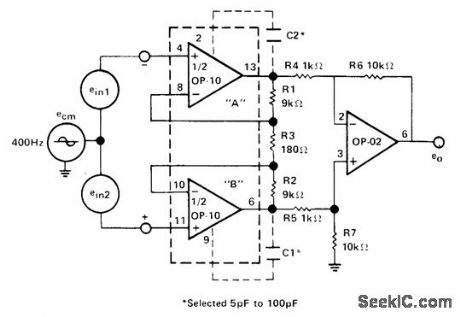
Precision Monolithics OP-10 dual opamp driving 0P-02 opamp gives high common-mode rejection ratio. CMRR is optimized by selecting C1 and C2 in range of 5 to 100 pF for minimum output e0 as viewed on CRO whilefeeding±10 V signal at 400 Hz to common connection of inputs.-''Linear &Conversion I.C.Products,''Precision Monolithics,Santa Clara,CA,1977-1978,p 15-2.
(View)
View full Circuit Diagram | Comments | Reading(565)
D_A_converter_in_unipolar_hookup_using_AD563_12_bit_D_A_converter_chip
Published:2009/7/20 4:25:00 Author:Jessie
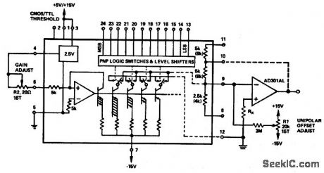
D/A converter in unipolar hookup using AD563 12-bit D/A converter chip(courtesy Analog Devices, Inc.). (View)
View full Circuit Diagram | Comments | Reading(796)
| Pages:877/2234 At 20861862863864865866867868869870871872873874875876877878879880Under 20 |
Circuit Categories
power supply circuit
Amplifier Circuit
Basic Circuit
LED and Light Circuit
Sensor Circuit
Signal Processing
Electrical Equipment Circuit
Control Circuit
Remote Control Circuit
A/D-D/A Converter Circuit
Audio Circuit
Measuring and Test Circuit
Communication Circuit
Computer-Related Circuit
555 Circuit
Automotive Circuit
Repairing Circuit