
Circuit Diagram
Index 875
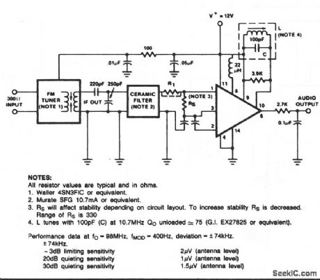
FM_MPX_SCA_RECEIVER
Published:2009/7/9 22:17:00 Author:May
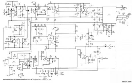
This receiver is capable of better than 1.5 μt VIHF sensitivity and uses MOSFET front-end circuitry with varactors to eliminate conventional bulky tuning capacitors. It also features high dynamic range, ceramic i-f filters requiring no alignment, and a quadrature-type detector with excellent limiting and AM rejection capability. The receiver operates from nominal 12-V supply. The kit is available from North Coun-try Radio, P.0. Box 53, Wykagyl Station, NY 10804. (View)
View full Circuit Diagram | Comments | Reading(1141)
2_watt_OTL_audio_power_amplifier_using_an_ECG1034
Published:2009/7/20 2:49:00 Author:Jessie
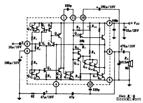
2-watt OTL audio power amplifier using an ECG1034. Recommended supply voltage is 12 volts. Typical voltage gain at 1 kHz is 50 dB. Input impedance is 20K. Frequency response is from 60 hertz to 50 kilohertz (courtesy GTE Sylvania Incorporated). (View)
View full Circuit Diagram | Comments | Reading(648)
VOLTAGE_FREEZER
Published:2009/7/9 22:17:00 Author:May
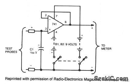
This circuit reads and stores voltages, thus freezing the meter reading even after the probes are removed. The op amp is configured as a unitygain voltage follower, with C1 situated at the input to store the voltage. For better performance, use an LF13741 or a TL081 op amp in place of the 741. These two are JFET devices and offer a much higher input impedance than the 741. (View)
View full Circuit Diagram | Comments | Reading(596)
ANALOG_DELAY_FLANGING_UNIT_
Published:2009/7/20 2:48:00 Author:Jessie
Audio from the guitar is fed first to a preamp and LP filter, then through an analog delay line IC. The delay is a function of clock frequency. The clock frequency, and, therefore, the delay time of the line, can be modulated by a low-frequency oscillator. This gives the characteristic sound to the guitar audio. (View)
View full Circuit Diagram | Comments | Reading(2071)
UHF_MOTION_DETECTOR
Published:2009/7/9 22:16:00 Author:May


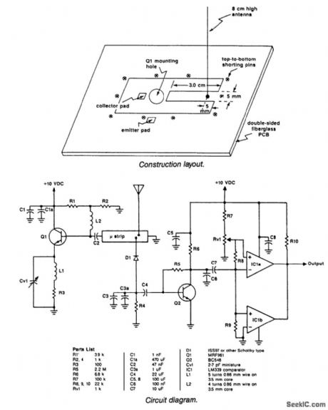
The UHF motion detector operates on the Doppler radar principle. Q1 is an oscillator that creates a adiated signal. An object in the radiated field reflects some of this energy back to the detector. If the ect is moving, the reflected signal will have a different frequency because of Doppler shift.Q1 is an oscillator coupled to a small (8-cm) antenna. This antenna also receives the reflected signal. D1 acts as a mixer and produces a beat note of frequency that is equal to the difference in reflected nd radiated signal. Q2 amplifies this signal and couples it to comparator/detector IC1A and IC1B. The utput can continue on to an alarm, relay, lamp,etc. (View)
View full Circuit Diagram | Comments | Reading(3629)
1_watt_OTL_audio_power_amplifier_using_an_ECG1032
Published:2009/7/20 2:48:00 Author:Jessie
1-watt OTL audio power amplifier using an ECG1032. Typical voltage gain at 1 kHz is 50 dB (courtesy GTE Sylvania Incorporated). (View)
View full Circuit Diagram | Comments | Reading(504)
DC_VOLTIETER
Published:2009/7/9 22:14:00 Author:May
This dc voltmeter, with high input resistance, uses a CA3130 BiMOS op amp and measures voltages from 10 mV to 300 V. Resistors R12 and R14 are used individually to calibrate the meter for full-scale deflection. Potentiometer R6 is used to null the op amp and meter on the 10-mV range by shorting the input terminals, then adjusting R6 for the first indication of upscale meter deflection. (View)
View full Circuit Diagram | Comments | Reading(1421)
CARRIER_CURRENT_RECEIVER_FOR_DATA_TRANSMISSION
Published:2009/7/9 22:12:00 Author:May
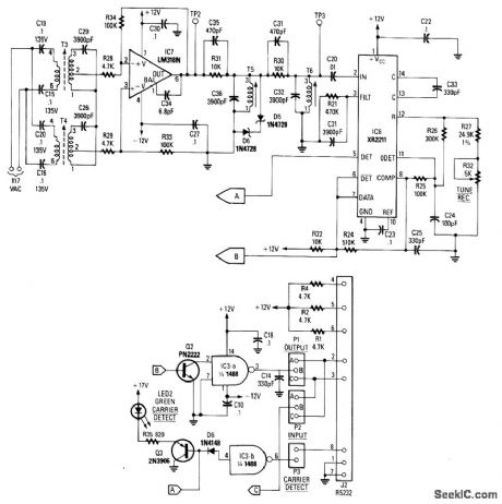
This receiver consists of an input network amplifier IC7 FSK PLL detector ICG, and output amplifier/ interface Q2, Q3, IC3A and IC3B, a 1488 Quad RS232 line driver of the carrier-current signal. Tuned amplifier IC7 amplifies this signal and drives PLL detector IC8. The values shown in the circuit are suitable for operation in the 100-kHz range. Recovered data at pins 5, 6, 7 is fed to the output amplifter/interface circuit (Fig, 6). This circuit is also used with the carrier-current data transmitter to form a pair. (View)
View full Circuit Diagram | Comments | Reading(1812)
KEYBOARD_MATRIX_INTERFACE
Published:2009/7/9 22:12:00 Author:May
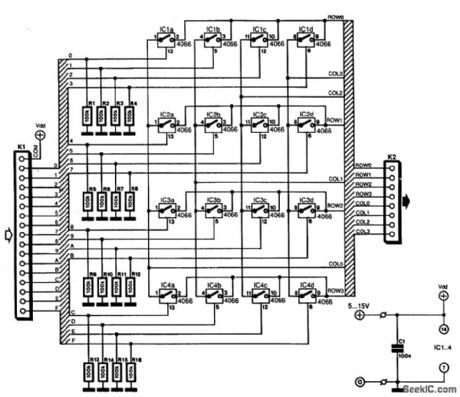
Keyboards can be slotted into two categories, at least as far as the manner that the switches are connected is concerned:those with a common connection and those with the switches arranged in a matrix.
The matrix type has the important advantage that the number of connections is an absolute minimum.Such an arrangement is ideal for ICs; many of these are designed for use with a matrix keyboard.
However, many keyboards are available in job lots, for instance, that apart from a common connection also have a connector for each key. Such keyboards can be connected to ICs that require a matrix type with the aid of a number of electronic switches.
The principle is straightforward: each key of the keyboard controls an electronic switch that is included in a matrix. As an example, the diagram shows a hexadecimal keyboard that is arranged in a 4-x-4 matrix. Each of the electronic switches is held in the open position by a pull-down resistor.
The current drawn by the circuit is very small and is determined mainly by the value of the pull-down resistors and the number of keys being pressed. The CMOS switches draw virtually no current. (View)
View full Circuit Diagram | Comments | Reading(1018)
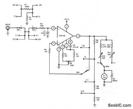
HIGH_INPUT_RESISTANCE_DC_VOLTMETER
Published:2009/7/9 22:12:00 Author:May
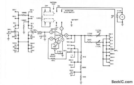
This voltmeter exploits a number of the CA3160 BiMOS op amp's useful characteristics. The available voltage ranges from 10 mV to 300 V. Powered by a single 8.4-V mercury battery, this circuit, with zero input, consumes approximately 500 μA. Thus, at full-scale input, the total supply current will increase by 1000 μA. (View)
View full Circuit Diagram | Comments | Reading(888)
CARRIER_CURRENT_TRANSMITTER_FOR_DATA_TRANSMISSION
Published:2009/7/9 22:09:00 Author:May


In this circuit, data at input C is amplified by IC2 and then fed to modulator IC1. IC1 generates two frequencies, depending on the values of C5, RIO, R3, R11, and R6. The frequency f, is generated if pin 9 IC1 is low and f2 if pin9lC1 is high. A square wave appears at pin 13 of IC1 and is fed to Q1, an amplifier stage, that is coupled via tuned transformer T, to the ac line via C1 and C2. Notice that, for safety reasons, C1 and C2 must be specifically rated for the ac line voltage. (View)
View full Circuit Diagram | Comments | Reading(887)
OVER_UNDER_VOLTAGE_MONITOR
Published:2009/7/9 22:09:00 Author:May

Any potential from 1 to 15 V can be monitored with this circuit. Two lamps alert any undesirable variation. The voltage differential from lamp turn-on to turn-off is about 0.2 V at any setting. High and low set points are independent of each other. The SCRs used in the circuit should be the sensitive gate type. R3 must be experimentally determined for the particular series of SCRs used. This is done by adjusting R3 to the point where the undervoltage lamp turns on when no signal is present at the SCR2 gate. Any 15-V segment can be monitored by putting the zener diode. D1. in series with the positive input lead. The low set-point voltage will then be the zener voltage plus 0.8 V. (View)
View full Circuit Diagram | Comments | Reading(815)
VERSATILE_ONE_SHOT_CPU_INTERFACE
Published:2009/7/9 22:09:00 Author:May

Process-control applications often require a monostable multivibrator (one-shot) with a pulse width that can be selected on-the-fly.
This circuit uses two CD4051B analog multiplexers to select the required timing components for the multivibrator, and hence, the pulse width. The multiplexers' address input comes from an 8-bit latch. Bit D6 tells the multivibrator whether to trigger on the leading or trailing edge of the trigger input. Bit D7 determines whether the multivibrator should be in a retriggerable or nonretriggerable mode. (View)
View full Circuit Diagram | Comments | Reading(646)
TWO_WIRE_INTERCOM
Published:2009/7/9 22:06:00 Author:May
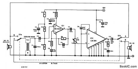
The design consists of an amplifier, a double-pole changeover switch and two loudspeakers:one forthe master station and one for the slave.More than one slave unit can be used,but each reqtures an additional changeover switch.
The power amplifier is a Type LM384,which can provide almost 2 W output at a supply voltage of 15V. Pins 3,4,5,10,11,and 12 are connected to ground and at the same time afford some coolling of thedevice,Because of that,the IC should not be fitted in a socket,but be soldered direct to the circuit board.
The LM384 processes signals with respect to earth so that an asymmetnc supply is sufficient.Theamplification has been set internally to×50(34 dB),The IC’s supply line is decoupled by C9.
To ensure adequate itiput sensitivity,a preamplifier,IC1,IS provided,which has an amplification of 11(21 dB).Because this stage IS intended for speech only, its bandwidth is limited to 160 Hz to 10 kHz.Divider R2/R3 at the input of the op amp is decoupled by C3.
Special loudspeakers that can also serve as microphones are readily available:in the prototype,MS-55units from Monacor were used,but a number of other makes will do Just db well.The bandwidth of the MS-55 (used db loudspeaker)extends from 150 Hz to 20 kHz and (used as a microphone)from 20 Hz to 20kHz,The MS-55 can handle up to 5-W output.To ensure satisfactory operation,particularly as a microphone,the loudspeaker must be fitted In a closed box.
Although it is advantageous for the microphone to have a low internal resistance,it is necessary for a transformer to be used at the input ofthe circuit,This has, however,the advantage that long cables canbe used.The present circuit uses a standard mains transformer instead of a special microphone trans-former. For this purpose,the secondary(6V) winding is connected to the microphone The microphone impedance is thereby magnified from about 8 Ω to around 10 kΩ.The power handling of thetransformer is quite high to ensure that signal losses in the primary winding are kept at a minimum. Capac-itor C1 suppresses HF interference.
If the mains transformer and the microphone transformer are housed in the same enclosure, some trial and error and screening are necessary to eliminate hum. The microphone transformer itself might cause hum in the remainder of the circuit. In that case, the preamp stage must also be screened.
In the prototype, the speech bandwidth was limited from 400 Hz to 4 kHz and this proved perfectly acceptable for good speech transfer. Most of the current drawn by the circuit flows through the power amplifier. At worst, this is 210 mA (680 mA peak), when the amplifier delivers 1.8-W output. The LM384 can deliver a power of up to 5 W. The supply voltage should then be raised to 22 V and a heatsm for the device will be necessary. (View)
View full Circuit Diagram | Comments | Reading(2014)
INVERTING_BISTABLE_BUFFER
Published:2009/7/9 22:02:00 Author:May
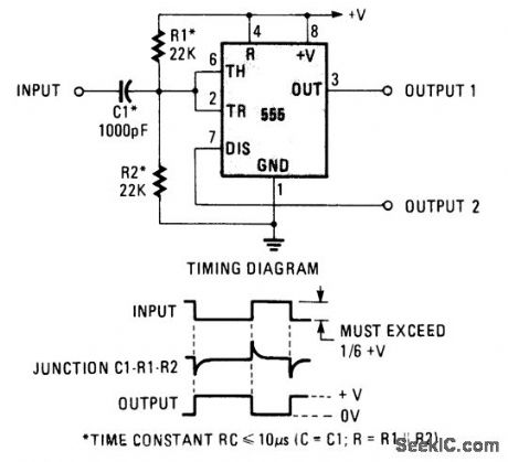
This circuit uses a 555 timer as a flip-flop bistable buffer. (View)
View full Circuit Diagram | Comments | Reading(616)
FM_TUNER
Published:2009/7/9 22:01:00 Author:May
View full Circuit Diagram | Comments | Reading(647)
PRECISION_INCREASING_BUFFER
Published:2009/7/9 22:01:00 Author:May
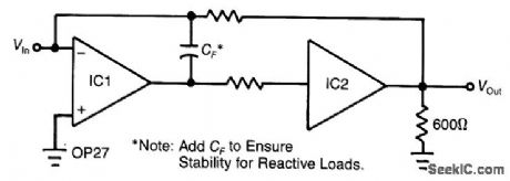
Adding an unity-gain buffer to your analog circuit can increase its precision. For example, by itself, the op amp IC1 exhibits a maximum dVOS/dT of 1.8 μA/℃ and can drive a 600-Ω load. Under thes, conditions, IC1 would dissipate 94 mW incrementally. Thus, the op amp's OJA of 150℃/W would change its VOS by 25μV.
The buffer, IC2, will isolate IC1 from the load and eliminate the change in power dissipation in IC1, thereby achieving 1C1's minimum, rated offset-voltage drive. The loop gain of IC1 essentially eliminates the offset of the buffer. Almost any unity-gain buffer will work, provided that it exhibits a 3-dB bandwidth that is at least 5 times the gain-bandwidth product of the op amp. (View)
View full Circuit Diagram | Comments | Reading(608)
AM_RADIO
Published:2009/7/9 22:00:00 Author:May
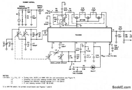
This circuit diagram is for a double-tuned, AM-channel, in-car radio receiver using the TEA5550. (View)
View full Circuit Diagram | Comments | Reading(6842)
INTEGRATOR_RAMP_GENERATOR_WITH_INITIAL_CONDITION_RESET
Published:2009/7/9 21:59:00 Author:May
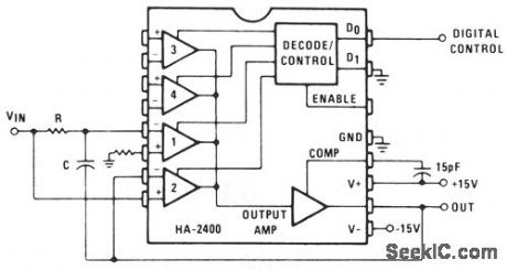
Channel 1 is wired as a conventional integrator, and channel 2 as a voltage follower. When channel 2 is switched on, the output will follow VIN and C will discharge to maintain 0 V across it. When channel 1 is then switched on, the output will initially be at the instantaneous value of VIN, and then will commence integrating towards the opposite polarity. This circuit is particularly suitable for timing ramp generation using a fixed dc input. Many variations, such as building programmable time constant integrators, are possible. (View)
View full Circuit Diagram | Comments | Reading(1334)
FULL-SCALE_FOUR_DECADE_3_1_2_DIGIT_DVM
Published:2009/7/9 21:59:00 Author:May
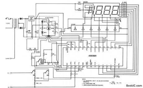
This DVM circuit uses a National ADD3501 DVM chip and an LM336 reference IC to create a simple DVM with relatively few components. When making a single range panel meter, the range switching components can be left out, as required. (View)
View full Circuit Diagram | Comments | Reading(2257)
| Pages:875/2234 At 20861862863864865866867868869870871872873874875876877878879880Under 20 |
Circuit Categories
power supply circuit
Amplifier Circuit
Basic Circuit
LED and Light Circuit
Sensor Circuit
Signal Processing
Electrical Equipment Circuit
Control Circuit
Remote Control Circuit
A/D-D/A Converter Circuit
Audio Circuit
Measuring and Test Circuit
Communication Circuit
Computer-Related Circuit
555 Circuit
Automotive Circuit
Repairing Circuit