
Circuit Diagram
Index 879
THREE_FREQUENCY_AUDIO_OSCILLATOR
Published:2009/7/20 4:20:00 Author:Jessie
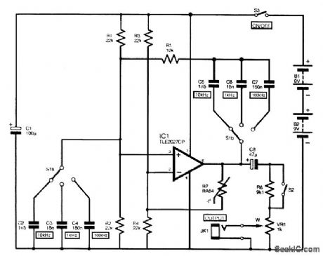
The full circuit diagram for the audio sine-wave generator is shown. Resistors R1 and R2 bias the noninverting (pin 3) input of IC1, and their parallel resistance forms one element of the Wien net-work. They are the equivalent of R1 in Fig. 1. The other resistor in the Wien network is R5. Three switched pairs of capacitors (C2 to C7) provide the unit with its three different output frequencies. Resistors R3 and R4 bias the inverting (pin 2) input of IC1, and their parallel resistance also acts as one element of the negative-feedback network. Thermistor R7 is the other section of the negative-feedback circuit. An RA53 thermistor is the normal choice for this application, but because of its lower cost, an RA54 is used in this circuit. Potentiometer VR1 is the variable-output attenuator. Opening switch S2 introduces losses through resistor R6 that reduce the output by about 20 dB. Use a value of 100 kΩ for R6 if a reduction by about 40 dB is preferred. (View)
View full Circuit Diagram | Comments | Reading(2457)
AC_CIRCUIT_BREAKER
Published:2009/7/9 21:19:00 Author:May
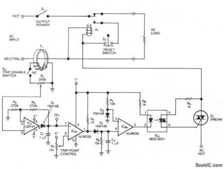
The adjustable circuit breaker responds in 0.02 s under all conditions-provided you select a fast relay for K1. For moderate overload conditions, it's preferable to use the fuse or the fast-acting breaker. Toroid transformer T1 senses ac load current and produces an ac signal at the wiper of R1, when switch S3 is closed. Diode D1 rectifies this signal to produce a positive voltage at test point TP1. Because R1 allows you to calibrate this voltage, the circuit accommodates a variety of current-sense transformers. To calibrate the trip threshold, apply the maximum expected overload and adjust R1 until the TP1 voltage is 0.7 V below the positive saturation level for IC1. Then adjust R4 for the desired trip point. To reset the circuit breaker after it has tripped, open S1 or S2. (View)
View full Circuit Diagram | Comments | Reading(2167)
5_watt_AF_power_amplifier_with_16_ohm_load_connected_to_supply
Published:2009/7/20 4:20:00 Author:Jessie
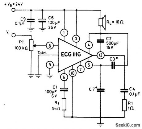
5-watt AF power amplifier with 16-ohm load connected to supply. Capacitor C3 is typically 330 pF and C7 is 1500 pF. Generally, C7 is five times greater than C3.The ECG1116 is a 12-pin QIP. To obtain the rated output heatsinking is necessary via the two tabs. Frequency response is from 40 hertz to 20 kilohertz. Input resistance is 5M (courtesy GTE Sylvania Incorporated). (View)
View full Circuit Diagram | Comments | Reading(722)
POWER_FAILURE_ALARM
Published:2009/7/9 21:17:00 Author:May
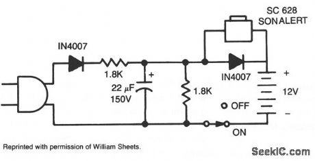
With power ac off, the alarm sounds when S1 is closed on. The 12-V battery is kept charged when the circuit is plugged in and the switch is left on. (View)
View full Circuit Diagram | Comments | Reading(0)
DUAL_POLARITY_15_V_SUPPLY
Published:2009/7/20 4:20:00 Author:Jessie
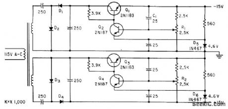
Output voltage is adjustable from 11 to15 v d-c and nearly constant from no load to 300 ma, or from 90 to 140 v ac line voltage.-D. T. Birch and K. E. Challis, Regulated Positive. Negative Supply Delivers Low-Voltage Direct Current, Electronics, 34:30, p 62. (View)
View full Circuit Diagram | Comments | Reading(581)
PHASE_MEASURING_AT_30_MC
Published:2009/7/20 4:19:00 Author:Jessie
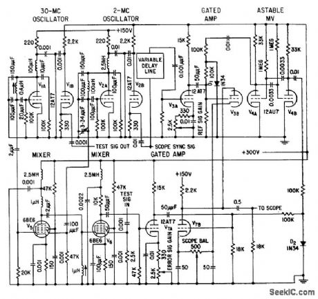
Double mixing process linearly transposes phase shifts accumulated at 30 Mc down to 2 Mc, where they are accurately compared against calibrated 2-Mc reference signal. Samples of 30-Mc and 2-Mc signals are mixed in V5, and 32-Mc sum frequency is then mixed with phase-shifted 30-Mc signal from unit under test by V6. Difference frequency, equal to 2 Mc plus phase shift, is amplified in V7A, fed through gate V7B, and associated circuits then superimpose this signal and that of 2-Mc reference oscillator on cro to get display of phase shift.-A. Nirenburg, How to Measure Midfrequency Phase Shift, Electronics, 31:35, p 46-47. (View)
View full Circuit Diagram | Comments | Reading(530)
VOLTAGE_LEVEL_INDICATOR
Published:2009/7/9 21:16:00 Author:May
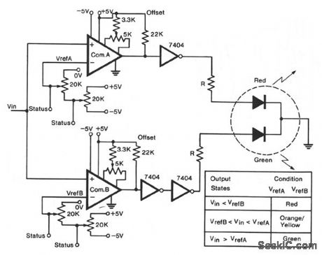
A tricolor LED, acts as the visual indicator of the voltage level. The voltage to be measured is connected to the two comparators in parallel. The first 20-KΩ trimmer defines a voltage between ±5 V and this becomes the full-scale value of the reference voltage. The second trimmer is a fine adjustment to give any reference voltage between 0 V and the full-scale voltage. Thus, it is possible to select both positive and negative reference voltages. During the initialization procedure, a voltage, equal to the reference voltage of each comparator, is connected to the input terminal, and the offset balance potentiometer is adjusted to give a reading between the high and low output voltage levels. The inverter following comp A ensures that, whatever the input voltage, at least one diode is lit. The two inverters following comp B leave the voltage largely unchanged, but provide the current necessary to illuminate the diode. The value of the resistance should be chosen so that the current through any single diode does not exceed the specified limit, usually 30 mA. The LED contains a red and a green diode with a common cathode. When both diodes are lit, a third color, orange, is emitted. With VREFA greater than VrefB, the output states given in the diagram apply. (View)
View full Circuit Diagram | Comments | Reading(0)
1_watt_cassette_record_playback_amplifiers_using_an_ECG1095_14_pin_DIP
Published:2009/7/20 4:19:00 Author:Jessie
1-watt cassette record/playback amplifiers using an ECG1095 14-pin DIP. The only external transistors outside of the EGG1095 are two EGG158s used for the AC bias circuit (courtesy GTE Sylvania Incorporated). (View)
View full Circuit Diagram | Comments | Reading(578)
VOLTAGE_LEVEL_INDICATOR
Published:2009/7/9 21:16:00 Author:May
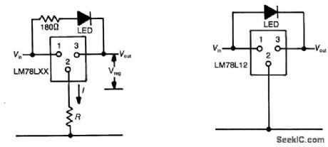
Three-terminal regulator device (LM78LXX) has Vout=Vin, until the input rises 1.5 to 2 V above the output when the regulated voltage Vreg = XX is obtained. A differential of 1.5 V between input and output is necessary to light the LED. Thus, the LED lights when Vin rises above Vreg + IR + 1.5 V, where I is typically 6 mA (a zener diode could be used in place of R). For input voltages much higher than necessary to light the LED, a current-limiting resistor in series might be necessary. A useful automotive application is shown in Fig. 14-9(b). The circuit indicates when battery voltage is above 13.5 V which indicates (in conjunction with gn ammeter) whether the alternator/regulator/battery system is operating correctly. With the engine off, the battery voltage drops to 12 V and the LED extinguishes. The circuit requires no calibration. (View)
View full Circuit Diagram | Comments | Reading(1513)
THREE_TONE_OSCILLATOR
Published:2009/7/20 4:18:00 Author:Jessie
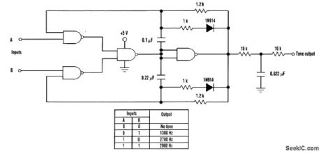
This TTL tone oscillator can generate one of three tones. The tone generation depends on the status of the two input control lines. The design consists of two standard TTL audio tone oscillators merged together using one 7400 TTL chip. Two input lines control the output status. With both inputs low, no output is generated. When input A is high, the high-tone oscillator is gated on. When input B is high, the low-tone oscillator is gated on. With both A and B high, both oscillators are gated on and the output tone generated is midway between the high and low tones. The 1N914 diode in series with a 1-kΩ resistor imposes a 50-percent duty cycle on the waveform. A low-pass filter on the output removes harmonics and mellows the output tone. (View)
View full Circuit Diagram | Comments | Reading(1740)
REGULATED_3_V_SUPPLY
Published:2009/7/20 4:18:00 Author:Jessie
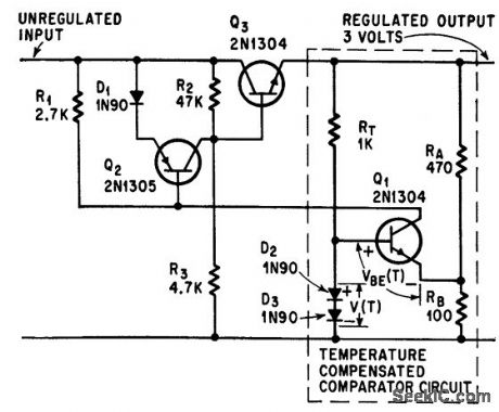
Junction diode D1 provides nonlinear voltage-current characteristic of tenor diode, as required for reference level below 2 v. Poor temperature characteristics of junction diode are offset by base-emitter voltage variation of transistor Q1 with temperature. Regulated output of 3 v within 2%, at 5 to 100 ma, is obtained from unregulated 4.8-v source over range of -16°C to +50°C.-A. K. Scidmore, Junction Diode Regulates Low-Voltage Supply, Electronics, 37:27, p 55-56. (View)
View full Circuit Diagram | Comments | Reading(642)
LINE_VOLTAGE_MONITOR
Published:2009/7/9 21:16:00 Author:May
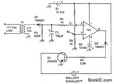
This circuit uses a type 741 op amp as a voltage comparator. One input of the 741 is connected to a reference voltage (a 12-V battery) through a resistor voltage divider. The potential at the noninverting input of the 741 is approximately 3 V. The inverting input of the op amp comparator is connected to the output of a line-operated 8-V power supply. When the ac power main fails, T1 will no longer be energized, so the charge stored in capacitor C1 will begin to discharge through resistor R5. When the capacitor voltage drops below the reference voltage of 3 V, the output of the comparator becomes high. This output condition will forward bias transistor Q1, causing the Sonalert to sound the alarm. The time constant of the R5/C1 combination is 22 seconds-long enough to prevent noise from triggering the alarm. (View)
View full Circuit Diagram | Comments | Reading(2508)
10_bit_D_A_converter_with_an_AD741_op_amp
Published:2009/7/20 4:18:00 Author:Jessie
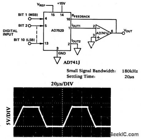
10-bit D/A converter with an AD741 op amp (courtesy Analog Devices, Inc.). (View)
View full Circuit Diagram | Comments | Reading(927)
AC_POWER_LINE_CONNECTIONS_MONITOR
Published:2009/7/9 21:14:00 Author:May
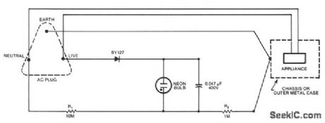
A continuous glow signiftes that everything is normal; a blinking or extinguished neon bulb indicates a broken earth-ground connection, or interchanged neutral and live wires. (View)
View full Circuit Diagram | Comments | Reading(812)
LARGE_SIGNAL_BUFFER
Published:2009/7/9 21:13:00 Author:May
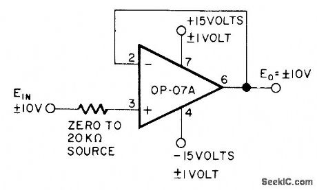
Unity-gain connec tion of Precision Monolithics 0P-07A opamp provides high accuracy (0.005% worst case) over temperature range of-55℃to + 125℃ for buffer applications for ±10 V signals.-D. Soderquist and G. Erdi, The OP-07 Ultra-Low Off-set Voltage Op Amp-a Bipolar Op Amp That Challenges Choppers, Eliminates Nulling, Precision Monolithics, Santa Clara, CA, 1975, AN13, p 8. (View)
View full Circuit Diagram | Comments | Reading(1729)
10_bit_DIA_converter_with_an_AD518_op_amp
Published:2009/7/20 4:17:00 Author:Jessie
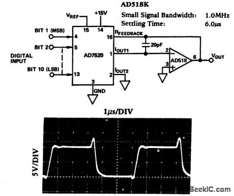
10-bit DIA converter with an AD518 op amp (courtesy Analog Devices, Inc.). (View)
View full Circuit Diagram | Comments | Reading(1003)
LOW_BATTERY_INDICATOR
Published:2009/7/9 21:13:00 Author:May
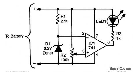
The sensing circuit consists of a 741 op amp set up as a voltage comparator, using a zener diode as a voltage reference. The op amp is inserted as a bridge between two resistance ladders, one which contains the zener reference, and the other a high-value linear potentiometer. When the voltage at the wiper of the potentiometer drops below the voltage set by the zener, the output of the op amp becomes low; that turns on the LED connected between it and VCC. The circuit can be adapted to work with battery-powered circuits that require between 6 and 18 V; the only changes needed would be a lower-voltage zener and a smaller current-limiting resistor in the case of voltage below 9 V, and a larger resistor for higher voltages. (View)
View full Circuit Diagram | Comments | Reading(0)
ELECTRIC_CROWBARS
Published:2009/7/9 21:13:00 Author:May

To avoid grief when using 12-V power supplies with mobile transceivers, especially when there is a short-circuit failure of the series pass transistor, crowbar circuits provide protection by clamping the power line and blowing the fuse within microseconds of an overvoltage condition. It is a good idea to incorporate the crowbar directly into the transceiver. The main difference between the two circuits is that less complex circuit B depends on component tolerances for the exact trigger level, while the circuit A includes a unijunction trigger to permit precise setting of the operating point. (View)
View full Circuit Diagram | Comments | Reading(905)
PROGRAMMABLE_AMPLIFIEIR
Published:2009/7/9 21:10:00 Author:May
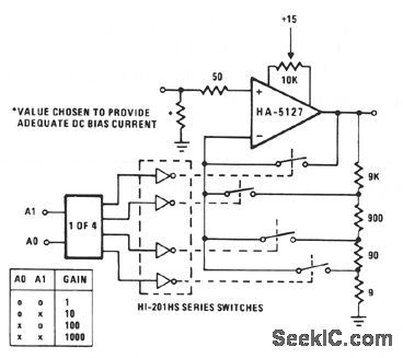
Often a circuit will be called upon to perform several functions. In these situations, the variable gain configuration of this circuit could be quite useful. This programmable gain stage depends on CMOS analog switches to alter the amount of feed-back, and thereby, the gain of the stage. Placement of the switching elements inside the relatively low-current area of the feedback loop, minimizes the effects of bias currents and switch resistance on the calculated gain of the stage. Voltage spikes can occur during the switching process, resulting in temporarily reduced gain because of the makebefore-break operation of the switches. This gain loss can be minimized by providing a separate voltage divider network for each level of gain. (View)
View full Circuit Diagram | Comments | Reading(629)
AUDIO_GENERATOR_CIRCUIT
Published:2009/7/20 4:17:00 Author:Jessie
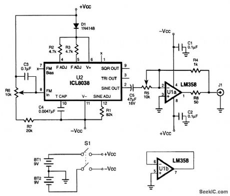
A very compact audio signal generator can be constructed using a precision waveform generator IC (ICL8038) made by Harris Semiconductor. This IC is unique in that it will generate three wave-forms: sine, triangle, and square waves. The frequency output is adjustable between 0.01 Hz and 300 kHz, and the sine-wave output distortion is less than 1 percent. The schematic diagram illustrates the application of the ICL8038 IC to construct a battery-powered mini-audio-signal generator that will provide 500 Hz to 1.5 kHz with adjustable-amplitude output. The output frequency of the generator is set by the combination of R2, R3, and (View)
View full Circuit Diagram | Comments | Reading(6690)
| Pages:879/2234 At 20861862863864865866867868869870871872873874875876877878879880Under 20 |
Circuit Categories
power supply circuit
Amplifier Circuit
Basic Circuit
LED and Light Circuit
Sensor Circuit
Signal Processing
Electrical Equipment Circuit
Control Circuit
Remote Control Circuit
A/D-D/A Converter Circuit
Audio Circuit
Measuring and Test Circuit
Communication Circuit
Computer-Related Circuit
555 Circuit
Automotive Circuit
Repairing Circuit