Amplifier Circuit
PROGRAMMABLE_AMPLIFIEIR
Published:2009/7/9 21:10:00 Author:May | From:SeekIC
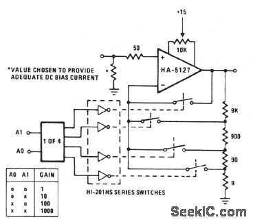
Often a circuit will be called upon to perform several functions. In these situations, the variable gain configuration of this circuit could be quite useful. This programmable gain stage depends on CMOS analog switches to alter the amount of feed-back, and thereby, the gain of the stage. Placement of the switching elements inside the relatively low-current area of the feedback loop, minimizes the effects of bias currents and switch resistance on the calculated gain of the stage. Voltage spikes can occur during the switching process, resulting in temporarily reduced gain because of the makebefore-break operation of the switches. This gain loss can be minimized by providing a separate voltage divider network for each level of gain.
Reprinted Url Of This Article:
http://www.seekic.com/circuit_diagram/Amplifier_Circuit/PROGRAMMABLE_AMPLIFIEIR.html
Print this Page | Comments | Reading(3)

Article Categories
power supply circuit
Amplifier Circuit
Basic Circuit
LED and Light Circuit
Sensor Circuit
Signal Processing
Electrical Equipment Circuit
Control Circuit
Remote Control Circuit
A/D-D/A Converter Circuit
Audio Circuit
Measuring and Test Circuit
Communication Circuit
Computer-Related Circuit
555 Circuit
Automotive Circuit
Repairing Circuit
Code: