
Circuit Diagram
Index 869
FOUR_QUADRANT_DIMMER
Published:2009/7/9 22:47:00 Author:May

This very special mains-operated dimmer for domestic or industrial lights is not available in proprie-tary form: it enables brightness control of two groups of lights in one operation. The possible combinations of brightness are shown itt the table. It will be clear that it is not possible to obtain continuous brightness control in the two groups. Instead, the circuit affords the setting of four states of brightness in either group: full on, fully dimmed, 1/3 on, and 2/3 on.
Both sections of the circuit operate on the well-known principle of the triac being switched from the blocking state to the conducting state with the aid of an RC network and a diode. The RC network provides the necessary phase shift and determines when the triac is switched. The rotary switch selects the resis-tor in a given network, and thus the brightness of the relevant group of lights. No resistor means that the group is off; a short-circuit gives maximum brightness, and resistors of 10 k0 and 18 k0 produce interme-diate brightness. The diodes prevent the groups from affecting one another.
The 64-μH choke (L1) and the 150 nF capacitor across the bridge rectifier prevent the dimmer caus-ing interference in other equipment connected to the mains.
If the triacs are fitted on a heatsink that is rated at 12°K/W, up to 500 W per group can be controlled.It is, of course, essential that the enclosure in which the dimmer is fitted provides ample cooling. A fair number of slots or holes in it are, therefore, essential; these should not permit the circuit elements to be touched.
The switch should have a nonmetallic spindle: this is not only safer than a metallic one, but it also enables the easy removal of the end-notch so that the switch can be rotated continuously, instead of having to be returned to the first stop every time it is operated.
The mains on/off switch S2 should be fitted with a built-in ON indicator bulb, which shows at a glance whether the circuit is on, even though S1 might be in the OFF position. Finally, remember that this circuit carries mains voltage in many places: good workmanship and insulation are, therefore, of the utmost importance. (View)
View full Circuit Diagram | Comments | Reading(960)
AUDIO_MILLIVOLTMETER
Published:2009/7/9 22:47:00 Author:May

Capacitor C4 couples the output of U1 to a simple attenuator, which is used to provide a loss of 0 dB, 20 dB, or 40 dB, depending on the setting of range switch S1. The circuits sensitivity is 10-V rms for fullscale deflection, so the attenuator gives additional ranges of 100-mV and 1-V rms. The attenuator output is connected through capacitor C5 to common-emitter amplifier Q1, which has a high-voltage gain of 40 dB.To get linear scaling on the meter, we have to use an active-rectifier circuit built around U2. That IC is connected so that its noninverting input is biased to the 0-V bus via R7. Capacitor C6 couples the output of Q1 to the noninverting input of U2; C7 is the compensation capacitor for U2.The voltage gain of U2 is set by the difference in resistance between the output and the inverting input, and between the inverting input and the ground bus. One resistance is made up of the diode-bridge rectifier D1 through D4, the other by resistor R8. This circuit has a nearly flat frequency response to about 200 kHz. (View)
View full Circuit Diagram | Comments | Reading(1292)
RESET_PROTECTION_FOR_COMPUTERS
Published:2009/7/9 22:46:00 Author:May
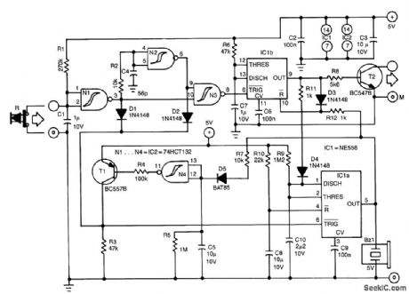
This protection circuit is inserted between the reset switch and the motherboard. The earth connection of the computer must be linked to terminal M of the protection circuit. The protection circuit can draw its power from the computer supply.
When the circuit has been fitted, operation of the reset switch will not immediately restart the computer. Instead, a buzzer will sound to alert you to the reset operation. The buzzer is actuated for 4 s by monostable IC1A, which is triggered by the reset switch. During these 4 s, the output, pin 5, of IC1A ensures that the reset function, pin 10, of IC1B is disabled. When the reset switch is operated again, monostable ICIB will be triggered and this starts the reset procedure. Transistor T2 is then switched on for 0.5 s and the buzzer is deactuated via R11 and D4.
The circuit around T1 and N4 ensures that IC1A can accept trigger pulses again 10 s after the mono time of IC1B has lapsed. This arrangement prevents, for example, children operating the reset switch. (View)
View full Circuit Diagram | Comments | Reading(1986)
TACHOMETERLESS_MOTOR_SPEED_CONTROL
Published:2009/7/9 22:44:00 Author:May


This provides bidirectional speed regulation for small motors and requires no tachometer. The volt-age that summing amplifier IC1A applies to the motor's windings equals:whereVCis the command voltage and IM is the motor current.If you set the motor's winding resistance and brush resistance(RM)equal to:the command voltage will be proportional to the motor winding's counter emf. C1 provides compen-sation. Set R1's value so that it equals 5 to 10% of RM's value. You can generally find RM's value in a motor's spec sheet. (View)
View full Circuit Diagram | Comments | Reading(498)
LINEAR_OHMMETER
Published:2009/7/9 22:44:00 Author:May

View full Circuit Diagram | Comments | Reading(1829)
CONTINUITY_TESTER
Published:2009/7/9 22:43:00 Author:May
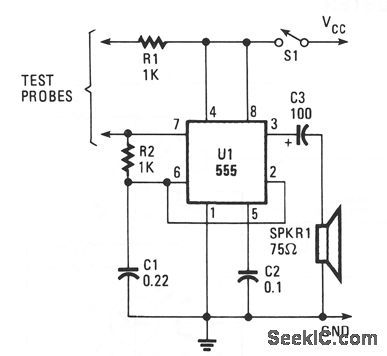
The continuity tester feeds a voltage throughthe positive probe to the circuit-under-test, whilethe negative probe serves as the return line. Voltage that rettion to the tester through the negative probe triggers circuit, giving an audible indication of continuity. (View)
View full Circuit Diagram | Comments | Reading(4294)
002_WEIGHING_ACCURACY
Published:2009/7/9 22:43:00 Author:May

Analog instrument covers up to 300 lb with resolution of 0.01 lb, for monitoring changes in body weight during clinical study. Bonded strain gages distributed symmetrically on platform of scale form bridge network R1-R2-R4-R5 serving as input for circuit that displays weight on digital panel meter and provides digital outputs to computer. Proper grounding is critical; all ground returns should go to single point at each powersupply common line. Article covers circuit operation in detain-J. Williams, This 30-PPM Scale Proves That Analog Designs Aren't Dead Yet, EDN Magazine, Oct. 5, 1976, p 61-64. (View)
View full Circuit Diagram | Comments | Reading(806)
DUAL_8051s_EXECUTE_IN_LOCK_STEP
Published:2009/7/9 22:43:00 Author:May

This hardware-software combination deletes clocks from the slave μP until both μPs synchronize. The firmware loop causes each μP to generate a WR signal once per loop. The circuit exclusive-0Rs the two WR signals to produce a miss-compare pulse. The miss-compare pulse latches into the two JK flip-flops via outputs LOCKSTP1 and LOCKSTP2. A high on these signals indicates that the μPs are in lock-step, causing both μPs' programs' execution to exit the firmware loop. If you use discrete components, you'll probably want to use the 0 output of the JK flip-flop and delete the circuit's inverters.
The listing uses the μPs' ports 1 and 3. You cannot use a memory-mapped location for the lock-stepdetect clear (K input) because this scheme would generate additional WR signals. You could apply this idea to other μPs, perhaps using their RD signals. This way, generating an RD signal to activate the lock-step-detect clear would not affect the synchronization inputs. (View)
View full Circuit Diagram | Comments | Reading(511)
VOLTAGE_MONITOR
Published:2009/7/9 22:42:00 Author:May

If the battery voltage exceeds about 11 V, current flows through R1, D1, and R2. The voltage produced as a result of current flow through R2 is sufficient to bias transistor Q1 into conduction. That places the collector voltage of Q1 virtually at ground. Therefore, Q2, driven fromthe collector of Q1, is cut off, LED1 and current-limiting resistor R4 are connected in the collector circuit of Q2. With Q2 in the cut-off state, the LED does not light. Should Q1's base voltage drop below approxi-mately 0.6 V. Q1 turns off. biasing Q2 on and illuminating LED1 to indicate that the battery voltage has fallen below the 11 V threshold level. (View)
View full Circuit Diagram | Comments | Reading(0)
UNIVERSAL_COMPANDER
Published:2009/7/9 22:41:00 Author:May

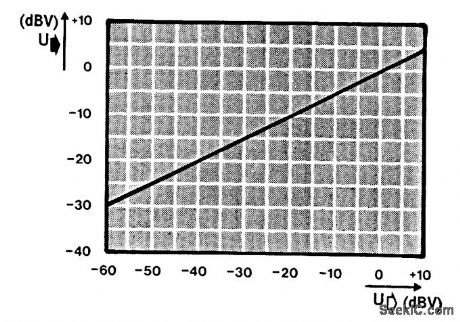
Signetics' type NE575 compander IC is intended primarily for use with battery power supplies of 3 to 7 V (max. 8 V). It draws a current of 3.5 mA at 3 V and 5 mA at 7 V. The compander process (compression at the input, expansion at the output) significantly improves the signal-to-noise ratio in a communications link.
The IC contains two almost identical circuits, of which one (pins 1 to 9) is arranged as an expander. The other (pins 11 to 19) can be used as expander, compressor or automatic load control (ALC), depend-ing on the externally connected circuit. For the compressor function, the inverting output of the internal summing amplifier is brought out to pin 12. This is not the case in the expander section, where a reference voltage is available at pin 8. This pin is interlinked to pins 1 and 19 to enable the setting of the dc operating point of the op amps.
The op amp in the expander section, pins 1 through 3, serves as output buffer in the compressor section, pins 17 through 19 as the input buffer. The IC has a relatively high output sensitivity and is evi-dently intended for processing small signals (microphone output level). A signal of 100 mV, for instance, is amplified by 1 only. The present circuit caters to larger input signals (line level); its maximum input level is 1.5 Vrms.
With a 1-V input into R13, a potential of about 500 mV exists between compressor output R7 and expander input R5. The compression characteristic is shown in Fig. 19-2(b). The signal range is reduced by about one half at the output, which is doubled in the expander. Thus, the range after compression and expansion is the same again, but that is not necessarily the case with the input and output level. The com-pander can be arranged to provide a constant attenuation or amplification. With the circuit values as shown in the diagram, the input and output levels are the same. The prototype had an overall gain of 0.5 dB when the expander input was connected directly to the compressor output.
To allow acceptance of high input levels, R13, R14, and the compressor input resistance form a 10:1 attenuator. At the expander input, R5 and the expander input impedance of about 3 k0 form a potential divider. If the compander is to be used with smaller signals, the attenuation can be reduced as appropriate. If the input level lies below 100 mV, R5, R13 and R14 can be omitted.
The compander covers the frequency range of 20 Hz to 20 kHz, the overall distortion is less than 1%, and the signal-to-noise ratio is about 80 dB. (View)
View full Circuit Diagram | Comments | Reading(1740)
CABLE_TESTER
Published:2009/7/9 22:40:00 Author:May

This compact tester checks cables for open-circuit or short-circuit conditions. A differential transistorpar at one end of each cable line remalns balanced as long as the same clock pulse generated bjy timer IC appears at both ends ofthe line. A clock pulse,just at the clock end of the line, lights a green LED,and aclock pulse,only at the other end,lights a red LED. (View)
View full Circuit Diagram | Comments | Reading(0)
LIGHT_DIMMER_SPEED_CONTROL
Published:2009/7/9 22:39:00 Author:May

A phase-controlled triac (HT-32) circuit provides control of effective voltage at load. Do not omit L1 and C4 because they are for RFI suppression. The maximum load is about 500W. WARNING: 120 Vac is present on this circuit-provide adequate insulation and construction techniques. (View)
View full Circuit Diagram | Comments | Reading(563)
DIODELESS_PRECISION_RECTIFIER
Published:2009/7/9 22:38:00 Author:May

A CA3130 BiMOS op amp, acts as an attenuator for positive inputs and as a conventional op amp fornegative signals. With 1-V rms input and a circuit gam of 0.8, its frequency response is -1%at 60 kHz and-1 dB at 300 kHz. (View)
View full Circuit Diagram | Comments | Reading(833)
SENSITIVE_RF_VOLTMETER
Published:2009/7/9 22:37:00 Author:May

This schematic shows a peak-reading diode voltmeter driven by two stages of amplification. A 100-μF capacitor provides a fairly large time constant, which results in satisfactory meter damping. The limited differential output voltage coupled with an overdamped meter prevents most needle pinning when you select an incorrect range position, or make other errors. An SPST toggle switch selects additional series resistance. This X2 function gives some more overlap of the sensitivity ranges. The resistance values shown are correct for use with a 100-μA meter with 1500-Ω internal resistance. (View)
View full Circuit Diagram | Comments | Reading(1409)
PRECISION_FULL_WAVE_RECTIFIER
Published:2009/7/9 22:37:00 Author:May
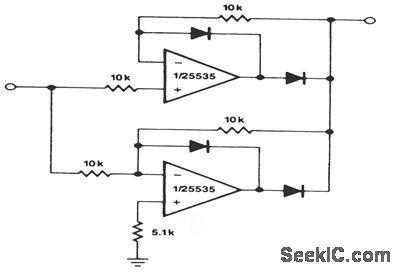
This circuit provides accurate full-wave rectification. The output impedance is low for both input polarities, and the errors are small at all signal levels. Note that the output will not sink heavy currents, except a small amount through the 10-KΩ resistors. Therefore, the load applied should be referenced to ground or a negative voltage. The reversal of all diode polarities will reverse the polarity of the output. Since the outputs of the amplifiers must slew through two diode drops when the input polarity changes, the 741-type devices give 5% distortion at about 300 Hz. (View)
View full Circuit Diagram | Comments | Reading(2029)
THREE_WAY_TOUCH_LAMP
Published:2009/7/9 22:37:00 Author:May
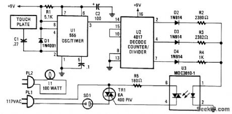
A three-way switch to control a lamp (off-dim-bright, etc.) uses an NE555 timer to generate a one-second pulse, triggered by ambient ac fields that are picked up by the human body. C1 and Dl form an input network. U2 is a decode counter/di ider and drives one of 10 outputs (three are used). The logic outputs drive various resistors in series with the LED in the optocoupler. The optocoupler controls a triac that is in series with a load (lamp, etc.).
By reconfiguring the outputs of U2, more than three brightness levels can be obtained, up to 10. An IN914 and resistor will be required for each output. (View)
View full Circuit Diagram | Comments | Reading(1248)
MINI_DRILL_CONTROL
Published:2009/7/9 22:36:00 Author:May


This circuit is intended as a revolution control for small dc motors as fitted, for instance, in small elec-tric drills (such as used for precision engineering and for drilling boards,among others). The behavior of these motors, which are normally permanent magnet types, is comparable to that of dependently pow-ered motors.In theory, the rpm of these motors depends solely on the applied voltage. The motor adjusts its rpm until the counter emf generated in its coils is equal to the applied voltage. There is, unfortunately, a drop across the internal resistance of the motor, which causes the rpm to drop in relation to the load. In other words, the larger the load, the larger the drop across the internal resistance and the lower the rpm.This circuit provides a kind of compensation for the internal resistance of the motor: when the urrent drawn by the motor rises, the supply voltage is increased automatically to counter the fall in rpm.The circuit is based on an enhanced voltage regulator that consists of IC1 and T1, which provides a easonably large output current (even small drills draw 2-to-5 A). The onset supply voltage, and thus the ram, is set by P2. Because of emitter resistance R1, the currents through IC1 and T1 will be related to one another in the ratio that is determined by R1 and R2. Owing to this arrangement, the internal short-circuit protection of IC1 will also, indirectly, provide some protection to T1.As soon as the current drawn exceeds a certain value, T2 will be switched on. This results in a base current for T3 so that R5 is in parallel (more or less) with R6. This arrangement automatically raises the output voltage to counter a threatened drop in rpm. The moment at which this action occurs is set by P1, so this circuit can be adapted pretty precisely to the motor used.If only very small motors are likely to be used, the power supply (transformer and bridge rectifier) can be rated more conservatively. As a guide, the current in the transformer secondary should be about 1.5 times the maximum dc output current. (View)
View full Circuit Diagram | Comments | Reading(2999)
INTEGRATED_AM_RECEIVER
Published:2009/7/9 22:33:00 Author:May


This circuit has aerial and local oscillator circuits for a 27-MHz recelver for remote control of garagedoors, projectors, curtains, etc. (View)
View full Circuit Diagram | Comments | Reading(1051)
FREQUENCY_SHIFT_KEYER
Published:2009/7/9 22:33:00 Author:May

Apply a signal to each differential amplifier input pair.When the gate voltage is changed from oneextreme to the other, the output can be switched alternately between the two input signals.When the gatelevel is high (1.5V), a signal applied between pms 5 and 6(channel A)will be passed and a signal appliedbetween pins 3 and 4(channel B)will be suppressed.In this manner,a binary-to-frequency conversion is obtained that is directly related to the binary sequence,which is driving the gate mput (pin 2). (View)
View full Circuit Diagram | Comments | Reading(544)
FET_VOLTMETER
Published:2009/7/9 22:31:00 Author:May

A2N3819 FET provides a solid-state VOM。The 2N3819 acts as a cathodefollowerin a VOM.The biasoffset(meter null) is obtained with R14 and R12 sets full-scale calibration R2 through R9 should totalabout10 MΩ.R10 is a protective resistor, and C2 provides ac bypassing to limit rf and noise pickup, (View)
View full Circuit Diagram | Comments | Reading(0)
| Pages:869/2234 At 20861862863864865866867868869870871872873874875876877878879880Under 20 |
Circuit Categories
power supply circuit
Amplifier Circuit
Basic Circuit
LED and Light Circuit
Sensor Circuit
Signal Processing
Electrical Equipment Circuit
Control Circuit
Remote Control Circuit
A/D-D/A Converter Circuit
Audio Circuit
Measuring and Test Circuit
Communication Circuit
Computer-Related Circuit
555 Circuit
Automotive Circuit
Repairing Circuit