
Circuit Diagram
Index 876
OSCILLATOR_BUFFERS
Published:2009/7/9 21:58:00 Author:May
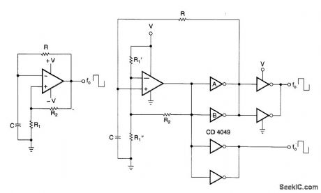
CM0S buffers added to an op amp oscillator improve performance, largely as a result of nonsymmetry and variability of the op amp's output saturation voitages. (View)
View full Circuit Diagram | Comments | Reading(870)
ACCURATE_RAMP_GENERATOR
Published:2009/7/9 21:57:00 Author:May
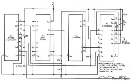
The ramp generator, an inexpensive alternative to commercial function generators, provides a more linear and repeatable output than conventional analog integrators. The circuit provides a triangle waveform in burst mode; in this case, two cycles of 10.24 ms each per input trigger pulse. IC4 is a dual monostable multi ibrator (one shot) in which the A side is configured as a latch (see Multivibrator IC performs extra tasks, EDN, September 6, 1984, p. 232). The rising edge of each input pulse triggers the B side, producing at pin 9 an output pulse whose duration depends on the timing capacitor's, CT, value-A 0.01-μF value gives a 500 μs pulse. This output provides a reset to the A side latch. While the latch is reset withQA, high, QA low, the other three ICs are active. The P1 through P6 connections, as shown, set oscillator IC2's frequency to 50 kHz at pin 11.Counter IC3 counts upward. The output at pin 11 of multifunction converter IC1 ramps up to fullscale, reverses, ramps down to zero, and then repeats this sequence of events. As this output completes its second cycle, IC3 reaches a count of 1024, causing the Q11 output to become high and toggle the IC4 latch. The resulting change of state on QA and QA resets the other three ICs, terminating further activity until the arrival of the next input trigger pulse. IC2 is included for its synchronous-reset capability, and it therefore drives the internal clock of IC1, which cannot be synchronously reset. Still IC2 can be omitted in some applications. The circuit operates from a 5-V supply. You can modify the output by changing IC2's frequency and IC3's output connection. (View)
View full Circuit Diagram | Comments | Reading(1028)
DIFFERENTIAL_TO_SINGLE_ENDED
Published:2009/7/9 21:55:00 Author:May
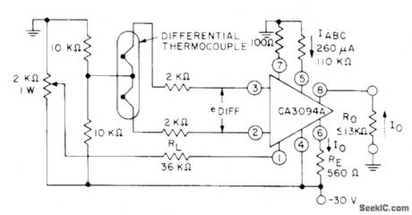
Conversion from differential input signal of thermocouple to single-ended output signal is achieved without feedback by using CA3094A programmable opamp. Output is ±4.7 V at 8.35 mA. Preamp gain is 180. For linear operation, differential input must be equal to or less than ±26 mV,- Circuit Ideas for RCA Linear ICs, RCA Solid State Division, Somerville, NJ, 1977, p 13. (View)
View full Circuit Diagram | Comments | Reading(1020)
4_1_2_DIGIT_DVM
Published:2009/7/9 21:55:00 Author:May
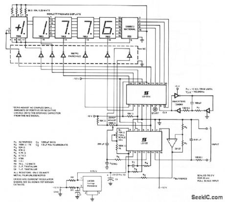
. 1-μV resolution.. Overrange blinking. 0-19.999 mV input voltages. Zero adjust-to-null offset introduced by PC board leakage and the comparator. (View)
View full Circuit Diagram | Comments | Reading(855)
GELGER_COUNTER
Published:2009/7/9 21:52:00 Author:May
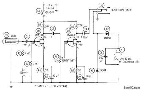
Output signal of Victoreen 1B85 G-M tube biased at 900 VDC is proportional to beta-gamma particle count. Signal is amplified by high-gain AF amplifier Q1-Q2 for driving AC meter circuit. Closed-circuit lack is provided for alternate use of headphones.Count-rate range of instrument is determined by exposing G-M tube to different calibrated radioactive samples and marking meter scale for each. Bias for counter can be obtained from three 300-V photoflashbatteries in series or equivalent supply capable of providing up to 10 mA.-R. P. Turner, FET Circuits, Howard W.Sams, Indianapolis, IN, 1977, 2nd Ed., p 152-153. (View)
View full Circuit Diagram | Comments | Reading(1387)
EXTENDED_COMMON_MODE_INSTRUMENT
Published:2009/7/9 21:51:00 Author:May
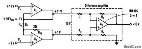
These circuits allow a larger common-mode range than most instrument amplifier inputs can allow. (View)
View full Circuit Diagram | Comments | Reading(677)
VOLTAGE_CONTROLLER_PULSE_WIDTH_GENERATOR
Published:2009/7/9 21:50:00 Author:May
View full Circuit Diagram | Comments | Reading(673)
INSTRUMENTATION_AMPLIFIER
Published:2009/7/9 21:49:00 Author:May
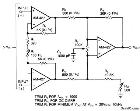
In a single difference amplifier Gonfiguration,the AM-427 exhibits common-mode rejection and spot noise voltage so low it is dominated by the resistor Johnson noise.The three-amplfier comfiguration shown avoids the low input-impedance characteristics of difference amplifiers.Because of the additional amplifiers used,the spectral noise volatge will increase from a typical of 3nV/Hz to approximately 4.9nV/Hz.The overall gain of the circuit is set at 1000;with balanced source resistors,a CMRR of 100dbis achieved. (View)
View full Circuit Diagram | Comments | Reading(0)
SCOPE_MIXER
Published:2009/7/20 4:12:00 Author:Jessie
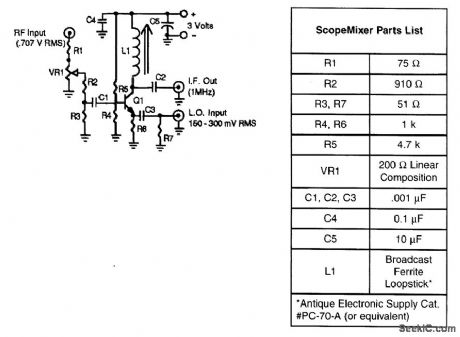
This circuit permits use of a low-frequency scope to view RF signals. The signal to be viewed is mixed with a LO signal about 1 MHz away and the IF output is viewed on the scope. (View)
View full Circuit Diagram | Comments | Reading(788)
CMOS_SHORT_PULSE_GENERATOR
Published:2009/7/9 21:48:00 Author:May
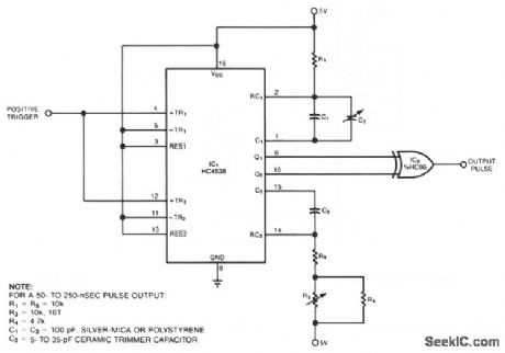
Comprising two low-power, CMOS chips, the pulse generator produces a precise pulse width in the 50 to 500 ns range. IC1 is a dual monostable multivibrator (one shot) in which each positive trigger pulse initiates simultaneous positive output pulses at pins 6 and 10. In response, XOR gate IC2 produces a positive pulse whose duration is equal to the difference between the two input-pulse durations. Section 1 of the one shot generates an approximate 1-μs reference pulse-shorter pulses are more susceptible to manu-facturing variations caused by parasitic layout capacitance. Variable capacitor C2 lets you adjust this pulse width. Section 2 of the one shot generates a variable-length pulse; you adjust its width by using potentiometer R3. Resistors R4 and R5 set the output pulse's maximum and minimum width, respectively. Because the XOR gate's rise and fall times are about 20 ns for reasonable values of load capacitance, you should calibrate the circuit using C2 for a minimum output-width of 50 ns. (View)
View full Circuit Diagram | Comments | Reading(1695)
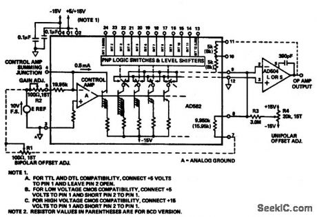
8_bit_D_A_converter_with_bipolar_output
Published:2009/7/20 4:12:00 Author:Jessie
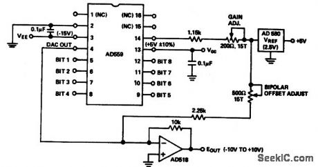
8-bit D/A converter with bipolar output (courtesy Analog Devices, Inc.). (View)
View full Circuit Diagram | Comments | Reading(998)
BURGLAR_ALARM_WITH_NC_AND_NO_SWITCHES
Published:2009/7/9 21:47:00 Author:May
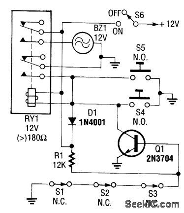
This circuit uses both NC and N0 sensors. Series NC sensors allow Q1 to activate RY1. NO sensors directly activate RY1. (View)
View full Circuit Diagram | Comments | Reading(721)
DUAL_SCOPE_ADAPTER
Published:2009/7/20 4:11:00 Author:Jessie
The input stage is the trigger amplifier based on the two channels of an LM319 dual comparator (IC1-a and IC1-b). The in-put signal is taken from the channel 1 output jack of your oscilloscope, and it is applied to J1 on the adapter. The input slope is selected by switch S1, and the signal is coupled to C3 and IC2, the multivibrator stage. Capacitor C3 provides the proper negative-going pulse to trigger IC2, a TLC555 CMOS timing IC. Switch S2 selects the desired range either milliseconds or mi-croseconds-and switch S3 selects the polarity of the output slope. Transistors Q1 and Q2 form a fast (less than 10-ns delay) inverting output stage. The output from switch S3 is ±5 V, which is sufficient for excellent contrast in intensity modulation. It is also satisfactory for stable triggering in the adapter's delayed-sweep mode. Precise input current to capacitors C4 and C5 is supplied from the collector of dual transistor Q3, a 2N5117. It is a dual-matched PNP pair in one package. Operational amplifier IC3, an LF356, is configured as a noninverting follower with gain. Transistor Q3 is configured as an unusual current mirror that unloads the relatively slow operational amplifier, allowing the second half of Q3 to demonstrate its fast dynamic response. A reference voltage is developed across both sets of emitter resistors (R20 to R25) to pro-duce the constant charging current for capacitors C4 and 05. The two sections of switch 54 (S4-a and S4-b) select the range-either 1.0, 10, or 100-in conjunction with switch S2 (milliseconds or microseconds). Zener diodes D6 and D7 permit the operational amplifier outputs to operate in their linear regions. Variable resistor R18 (1 kΩ, 10 turns) is the range multiplier. (View)
View full Circuit Diagram | Comments | Reading(1909)
PICOAMMETER
Published:2009/7/9 21:46:00 Author:May
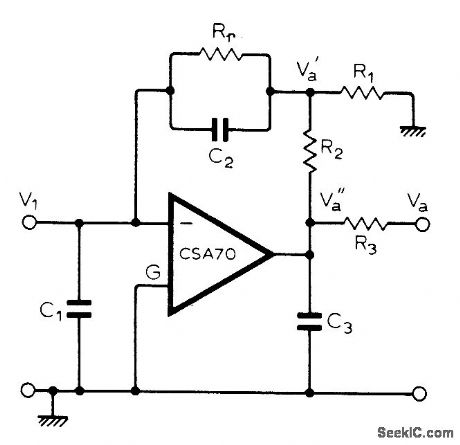
Highly stable circuit uses Valvo CSA70 chopper-stabilized opamp. Required high feedback resistance is provided by R1-R2 in feedback loop. Article gives design equations.Rr' andR2 are 1 megohm, R1 is 10 ohms, and all capacitors are 0.1 μF.-K. Kraus, High-Speed Picoammeter, Wireless World, May 1976,p 78. (View)
View full Circuit Diagram | Comments | Reading(3141)
D_A_converter_in_bipolar_hookup_using_an_AD563
Published:2009/7/20 4:11:00 Author:Jessie
D/A converter in bipolar hookup using an AD563 (courtesy Analog Devices, Inc.). (View)
View full Circuit Diagram | Comments | Reading(1243)
SIMPLE_BURGLAR_ALARM_WITH_NC_SWITCHES
Published:2009/7/9 21:46:00 Author:May
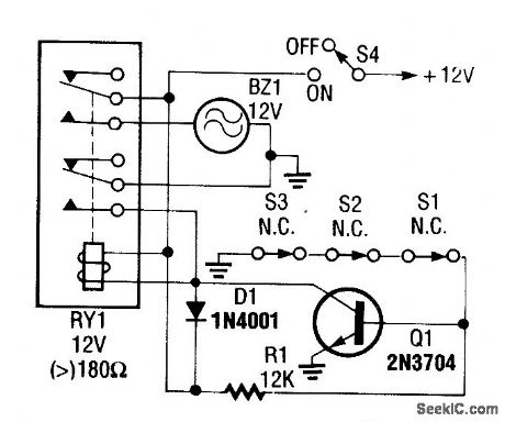
This relay draws 1 mA of idling current. Q1 detects open switch and energizes RY1. (View)
View full Circuit Diagram | Comments | Reading(672)
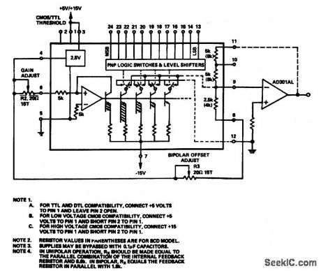
D_A_converter_in_unipolar_and_bipolar_hookup
Published:2009/7/20 4:10:00 Author:Jessie
D/A converter in unipolar and bipolar hookup (courtesy Analog Devices, Inc.). (View)
View full Circuit Diagram | Comments | Reading(902)
10_bit_D_A_converter_with_±5_volt_buffered_bipolar_output
Published:2009/7/20 4:09:00 Author:Jessie
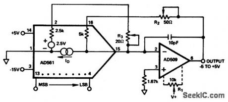
10-bit D/A converter with ±5-volt buffered bipolar output (courtesy Analog Devices, Inc.). (View)
View full Circuit Diagram | Comments | Reading(947)
10_bit_D_A_converter_with_unbuffered_±166_volt_bipolar_output
Published:2009/7/20 4:08:00 Author:Jessie
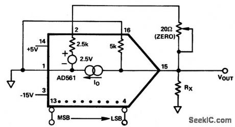
10-bit D/A converter with unbuffered ±1.66-volt bipolar output (courtesy Analog Devices, Inc.). (View)
View full Circuit Diagram | Comments | Reading(848)
WIDE_RANGING_PULSER
Published:2009/7/9 21:46:00 Author:May
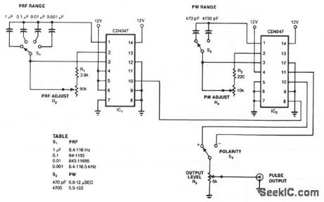
An output pulse's characteristics depend upon two multivibrator's timing components. IC1's free-running astable-mode frequency sets the pulse's prf, whereas the pulse's width comes from IC2's monostable operation. (View)
View full Circuit Diagram | Comments | Reading(676)
| Pages:876/2234 At 20861862863864865866867868869870871872873874875876877878879880Under 20 |
Circuit Categories
power supply circuit
Amplifier Circuit
Basic Circuit
LED and Light Circuit
Sensor Circuit
Signal Processing
Electrical Equipment Circuit
Control Circuit
Remote Control Circuit
A/D-D/A Converter Circuit
Audio Circuit
Measuring and Test Circuit
Communication Circuit
Computer-Related Circuit
555 Circuit
Automotive Circuit
Repairing Circuit