
Circuit Diagram
Index 864
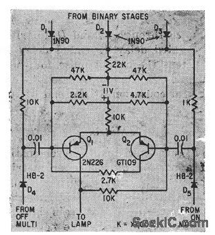
MAGNETIC_DRUM_READ_AMPLIFIER
Published:2009/7/20 2:01:00 Author:Jessie
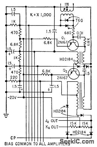
Amplifies phase-modulated step-modulated Manchester signal from magnetic drum read head and provides phase detection for recovery of stored information. Also used for synchronization.-A. J. Strassman and R. E. Keeter, Clock Track Recorder For Memory Drum, Electronics, 32:41, p 74-76. (View)
View full Circuit Diagram | Comments | Reading(490)
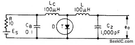
INDUCTIVE_LOAD_TRIAC_SWITCH
Published:2009/7/9 23:20:00 Author:May
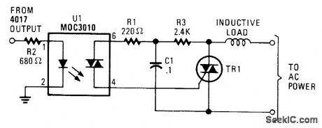
An additional resistor and capacitor enable control of an inductive load, such as a small blower motor, fluorescent lamp, etc. (View)
View full Circuit Diagram | Comments | Reading(1706)
TIME_OUT_WARNING
Published:2009/7/20 2:01:00 Author:Jessie
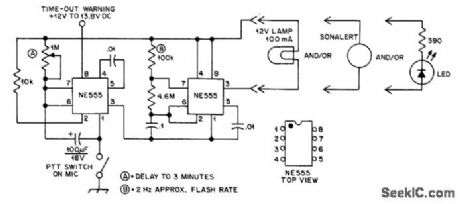
Provides either visual or audible warning after preset interval up to 3 min, when pin 1 of first NE555 is grounded by push-to-talk switch on microphone of mobile transmitter. When preset limit is reached, pin 3 provides ground for second NE555 that makes it pulse at 2-Hz rate to warn that time limit for use of repeater is being approached.-F. Sharp, Time-0ut Warning, QST, 0ct. 1976, p 67. (View)
View full Circuit Diagram | Comments | Reading(612)
DIGITAL_LEVELS_SCOPE_DISPLAYS_2_LOGIC_SIGNALS_ON_1_SCOPE
Published:2009/7/9 23:19:00 Author:May
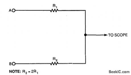
Using this simple resistor circuit, you can trick your oscilloscope into displaying two logic signals on one channel. If you select R2 to be twice R1, the scope trace will show one of four distinct analog levels for each possible combination of the states of inputs A and B.
Of course, the voltage levels that your oscilloscope sees depends heavily on the current-sourcing capability of your digital logic. Because you must use high resistances, this technique has a limited frequency range. (View)
View full Circuit Diagram | Comments | Reading(437)
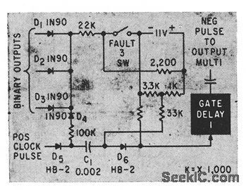
FAULT_SENSING_SWITCH
Published:2009/7/9 23:19:00 Author:May
When fault in microwave system has effect of closing switch 3, gated delcty shortens output pulse for that function when binary input signals are negative.-J. B. Bullock, Pulse-Coded Fault Alarm in Microwave Systems, Electronics, 33:1, p 82-84. (View)
View full Circuit Diagram | Comments | Reading(682)
SINE_WAVE_TUNNEL_DIODE
Published:2009/7/20 2:01:00 Author:Jessie
Low-impedance capacitor in parallel with sefies-resonant circuit of tunnel-diode relaxation oscillator passes all frequencies except that for series resonance, giving sinusoidal voltage across output capacitor. Output frequency varies from Q1 to 0.8 Mc over bias range of 000 to 400 mv.-Wen-Hsiung Ko, Designing Tunnel Diode Oscillators, Electronics, 34:6, p 68-72. (View)
View full Circuit Diagram | Comments | Reading(1089)
FLIP_FLOP_DEBOUNCER_SWITCH
Published:2009/7/9 23:19:00 Author:May
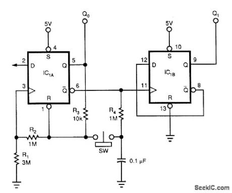
Although this circuit uses a 74HC74, any CMOS variant of this flip-flop will work. IC1A acts as a true/ complement buffer. RI and R2 ensure that IC1A comes out of reset before the clock's edge occurs. R3 applies IC1A's logic state to pins 1 and 3. When the switch closes, the next logic state stored on the capaci-tor transfers to the flip-flop's reset and clock inputs. Releasing the switch lets the capacitor charge to the next state via R4. IC1A's output is the LSB; IC1B's output is the MSB.
Notice that the counter's state advances when the switch is first pressed, rather than when it's released; the latter is the case with many other switch-debouncing schemes. lbu can replace RI with a 22-pF capacitor to reduce the circuit's sensitivity to parasitic effects. The addition of this capacitor also lets you !ower the magnitude of R2 and R3 by a factor of 10. (View)
View full Circuit Diagram | Comments | Reading(2912)
100_MC_COLPITTS
Published:2009/7/20 2:00:00 Author:Jessie
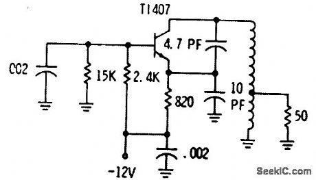
Uses conventional bipolar transistor, which has low noise in operation from low-impedance voltage generator. Temperature drift is much greater than with fet. -Fets Come Alive: Clinic Unveils Practical Circuits, EEE, 14:4, p 16-18. (View)
View full Circuit Diagram | Comments | Reading(707)
dc_MOTOR_SPEED_CONTROL
Published:2009/7/9 23:18:00 Author:May
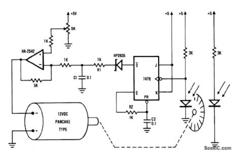
The system shown consists of the HA-2542, a small 12-Vdc motor, and a position encoder. During operation, the encoder causes a series of constant-width pulses to charge C1. The integrated pulses develop a reference voltage, which is proportional to motor speed and is applied to the inverting input of HA-2542. The noninverting input is held at a constant voltage, which represents the desired motor speed. A difference between these two inputs will send a corrected drive signal to the motor, which completes the speed control system loop.
(View)
View full Circuit Diagram | Comments | Reading(0)
SIMPLIFIED_VOLTAGE-LEVEL_SENSOR
Published:2009/7/9 23:18:00 Author:May
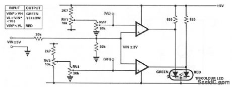

This circuit uses only one IC, either 1, LM393 dual comparator or 1/2, LM339 quad comparator. RV1 and RV3 set the full scale reference voltage, and RV2 and RV4 set the switching thresholds to a value between 0 V and the full-scale reference. The change in input voltage needed to fully switch the output state is less than 0.05 mV (typical). (View)
View full Circuit Diagram | Comments | Reading(1287)
TUBE_REPLACES_180°_TRANSFORMER
Published:2009/7/20 2:39:00 Author:Jessie
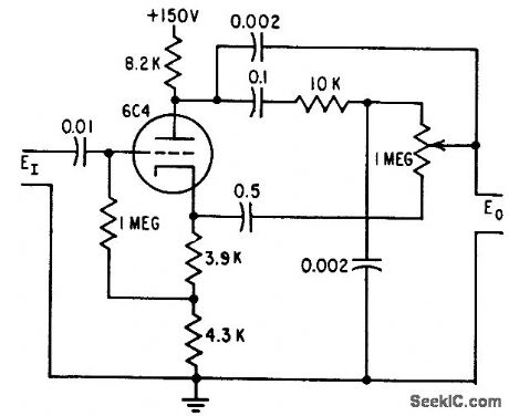
Elimination of transformer resonance effects at higher frequencies permits phase shifter to handle wider band of frequencies, from 500 to 2,000 cps for component values shown.-W. G. Shepard, Phase Shifter Range Exceeds 180°, Electronics, 31:19, p 96-100. (View)
View full Circuit Diagram | Comments | Reading(534)
SIREN_WARBLE_GENERAIOR
Published:2009/7/9 23:18:00 Author:May

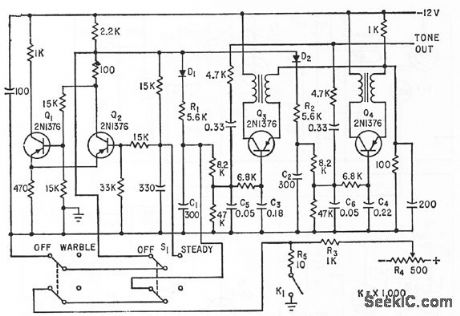
Genemtes singletone and wcrble signals. Blocking oscillators Q3 and Q4, having slightly different frequendes, are frequency-modulated by triangular-wave output of low-frequency mvbr Q1-Q2, to produce siren-type wail.-W. F. Ferguson, High-Powered Audio Alarm Systems, Eleeronics, 33:16, p 70-72. (View)
View full Circuit Diagram | Comments | Reading(686)
FM_ratio_detector_circuit
Published:2009/7/20 2:39:00 Author:Jessie
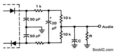
FM ratio detector circuit. With R equal to 22K and C equal to 100 pF the roll off occurs at about 70 kHz (courtesy Motorola Semiconductor Products Inc.). (View)
View full Circuit Diagram | Comments | Reading(2084)
XOR_GATE
Published:2009/7/9 23:15:00 Author:May
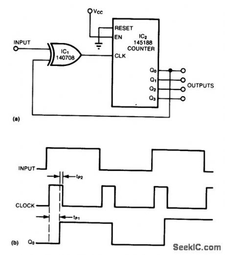
Inverting the negative-going input transactions allows the counter to count both positive- and negative-going edges. The XOR gate transforms the input signal into a series of short pulses whose width is equal to the sum of the counter and gate propagation delays. (View)
View full Circuit Diagram | Comments | Reading(1142)
PHASE_SHIFTER_WITH_LINEAR_BIASING
Published:2009/7/20 2:38:00 Author:Jessie
Frequency range of more than two decades can be obtained from voltage-controlled oscillator when linear biasing is used for phase-shift circuit.-R. A. Greiner and S. K. Morgan, Voltage Controlled Wide-Range Oscillator, Electronics, 34:51, p 31-35. (View)
View full Circuit Diagram | Comments | Reading(827)
CODER_MATRIX
Published:2009/7/9 23:15:00 Author:May
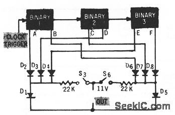
Circuit shows portion of coder matrix associated with microwave system false alarm circuits, having switches 53 and 56.-J. B. Bullock, Pulse-Coded Fauh Alarm in Microwave Systems, Electronics, 33:1, p 82-84. (View)
View full Circuit Diagram | Comments | Reading(522)
SAMPLE_AND_HOLD_2
Published:2009/7/9 23:15:00 Author:May
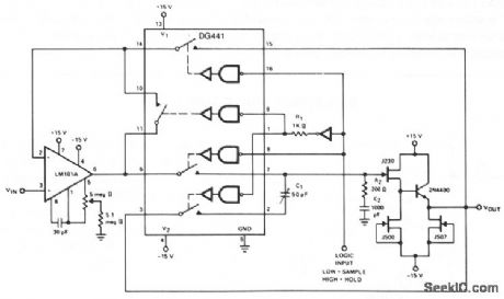
The LM101A provides gain and buffers the input from storage capacitor C2. R2 adds a zero in the open loop response to compensate for the pole caused by the switch resistance and C2, improving the closed-loop stability. R1 provides a slight delay in the digital drive to pins 1 and 9. C1 provides cancellation of coupled charge, keeping the sample-and-hold offset below 5 mV over the analog signal range of -10 through + 10 V. Aperture time is typically 1 pts, the switching time of the DG441. Acquisition time is 25 μs, but this can be improved by using a faster slewing op amp. Droop rate is typically less than 5 mV/s at 25℃. (View)
View full Circuit Diagram | Comments | Reading(739)
AUTOMATIC_LIGHT_BULB_CHANGER
Published:2009/7/9 23:15:00 Author:May
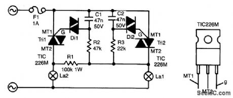
The circuit presented here guarantees that if bulb La1 gives up the ghost, bulb La2 will take over its task. In series with La1 is triac Tri2. Resistor R3 and C2 form a delay network. As soon as the voltage across C2 rises above about 30 V, diac (gateless triac) D2 is switched on, which causes Tri2 to conduct so that La1 lights.
The control circuit of La2 is parallel to that of La1, but because R2/C1 has twice the delay of R3/C2, Tri1 will not be triggered when Tri2 conducts; C1 discharges so that Tri1 cannot be triggered.
When, however, La1 is open-circuited, a voltage is across both RC networks via La2 and RI. Again, Tri2 will be triggered first, but because the current is smaller than its holding current, it will cease to conduct almost immediately. Capacitor C1 will then continue to charge and after a little while Tri1 is switched on.
Because the time constant for La2 is somewhat longer than that for La1, La2 will always be slightly less bright than La1. It is, of course, possible to give La2 a slightly higher wattage than La1 to ensure equal brightness.
Without heatsinks, the triacs can handle up to 100 W each; with heatsinks, powers of up to 1 000W can be accommodated. It is not recommended to use bulbs with a wattage below 25W, because these can flicker.
The triacs can be any type that can handle at least 400 V at no less than 5A. The M types used in the prototype can handle 600 V at 5A. (View)
View full Circuit Diagram | Comments | Reading(1863)
CHILD_PROOF_RESET_SWITCH
Published:2009/7/9 23:14:00 Author:May
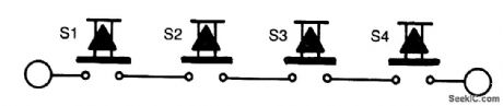
The reset switch on a computer is very important. If an operating instruction threatens to wreck the internal management of a computer, the reset button is often the only way of avoiding a possible disaster. On the other hand, it also could cause a disaster.
It is particularly important that children or pets cannot inadvertently operate the control. The circuit proposed here should put an end to your worries in this respect. Instead of one reset switch, it is necessary to press four switches simultaneously. The chances of this happening via accident, child, or pet are negligible.
The four switches are placed in positions that make it impossible to operate them all with one hand.Instead, two of them can be operated with the fingers of one hand and the other two with the fingers on the other hand. As shown, the four switches are connected in series and are intended to replace the exist-ing switch. (View)
View full Circuit Diagram | Comments | Reading(577)
4_channel_SQ_logic_decoder
Published:2009/7/20 2:38:00 Author:Jessie

4-channel SQ logic decoder. Current drain at 20 volts is 60 mA. Input impedance is 2M. Output impedance is 2K (courtesy GTE Sylvania Incorporated). (View)
View full Circuit Diagram | Comments | Reading(570)
| Pages:864/2234 At 20861862863864865866867868869870871872873874875876877878879880Under 20 |
Circuit Categories
power supply circuit
Amplifier Circuit
Basic Circuit
LED and Light Circuit
Sensor Circuit
Signal Processing
Electrical Equipment Circuit
Control Circuit
Remote Control Circuit
A/D-D/A Converter Circuit
Audio Circuit
Measuring and Test Circuit
Communication Circuit
Computer-Related Circuit
555 Circuit
Automotive Circuit
Repairing Circuit