Switch Control
FLIP_FLOP_DEBOUNCER_SWITCH
Published:2009/7/9 23:19:00 Author:May | From:SeekIC

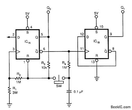
Although this circuit uses a 74HC74, any CMOS variant of this flip-flop will work. IC1A acts as a true/ complement buffer. RI and R2 ensure that IC1A comes out of reset before the clock's edge occurs. R3 applies IC1A's logic state to pins 1 and 3. When the switch closes, the next logic state stored on the capaci-tor transfers to the flip-flop's reset and clock inputs. Releasing the switch lets the capacitor charge to the next state via R4. IC1A's output is the LSB; IC1B's output is the MSB.
Notice that the counter's state advances when the switch is first pressed, rather than when it's released; the latter is the case with many other switch-debouncing schemes. lbu can replace RI with a 22-pF capacitor to reduce the circuit's sensitivity to parasitic effects. The addition of this capacitor also lets you !ower the magnitude of R2 and R3 by a factor of 10.
Reprinted Url Of This Article:
http://www.seekic.com/circuit_diagram/Control_Circuit/Switch_Control/FLIP_FLOP_DEBOUNCER_SWITCH.html
Print this Page | Comments | Reading(3)

Article Categories
power supply circuit
Amplifier Circuit
Basic Circuit
LED and Light Circuit
Sensor Circuit
Signal Processing
Electrical Equipment Circuit
Control Circuit
Remote Control Circuit
A/D-D/A Converter Circuit
Audio Circuit
Measuring and Test Circuit
Communication Circuit
Computer-Related Circuit
555 Circuit
Automotive Circuit
Repairing Circuit
Code: