
Circuit Diagram
Index 878
BURGLAR_ALARM_WITH_TIMED_SHUTOFF
Published:2009/7/9 21:36:00 Author:May
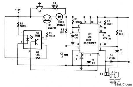
When S1 (sensor) is closed, power is applied to U2, a dual timer, After a time determined by C2, C1 is energized after a predetermined time determined by the value of C5, pin 9 of U2 becomes low, switching off the transistor in the optoisolater, cutting anode current of SCR1 and de-energizing K1. The system is now reset. Notice that (R6× C2) is less than (R7× C5). The ON time is approximately given by:
(R7×C5)-(R6×C2))=tON (View)
View full Circuit Diagram | Comments | Reading(1546)
8_bit_D_A_converter_with_voltage_output_and_using_a_fixed_reference
Published:2009/7/20 4:24:00 Author:Jessie
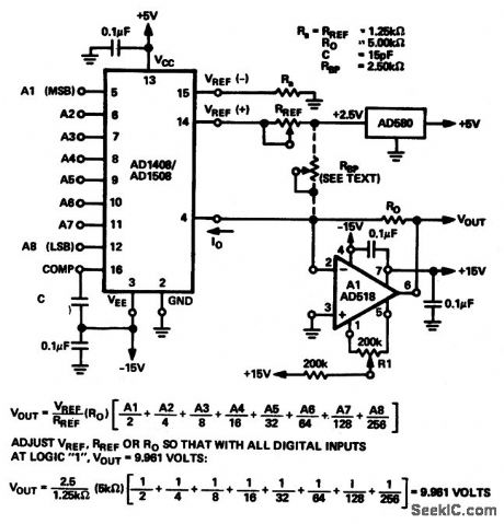
8-bit D/A converter with voltage output and using a fixed reference. For RREF at 1k,2.5k or 5k the minimum value of C should be 15 pF,37 pF or 75 pF respectively(courtesy Analog Devices, Inc.). (View)
View full Circuit Diagram | Comments | Reading(1025)
SELF_LATCHING_BURGLAR_ALARM
Published:2009/7/9 21:31:00 Author:May
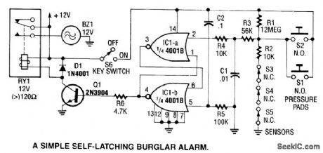
This alarm uses IC1A and IC1B as a latch. When sensors S1 through S5 activate, IC1A turns on and forces IC1B to cut off. Q1 drives RY1. (View)
View full Circuit Diagram | Comments | Reading(890)
10_bit_DIA_converter_with_an_AD505_op_amp
Published:2009/7/20 4:23:00 Author:Jessie
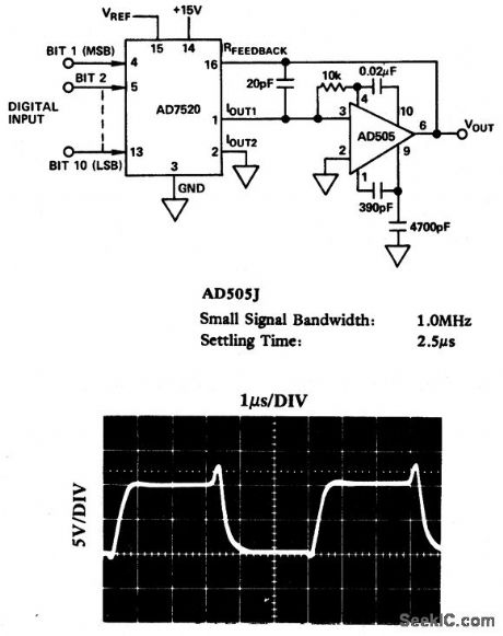
10-bit DIA converter with an AD505 op amp (courtesy Analog Devices, Inc.). (View)
View full Circuit Diagram | Comments | Reading(931)
300_V_200_MA_REGULATOR
Published:2009/7/20 4:23:00 Author:Jessie
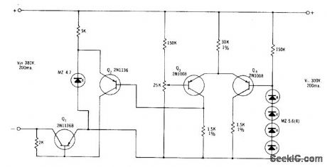
Transistor Q1 serves as series element in negative lead of high-voltage regulated supply, dissipating less than 16 w. Zener Diode Handbook, International Rectifier Corp., 1960, p 58. (View)
View full Circuit Diagram | Comments | Reading(680)
OSCILLOSCOPE_PREAMP
Published:2009/7/9 21:30:00 Author:May
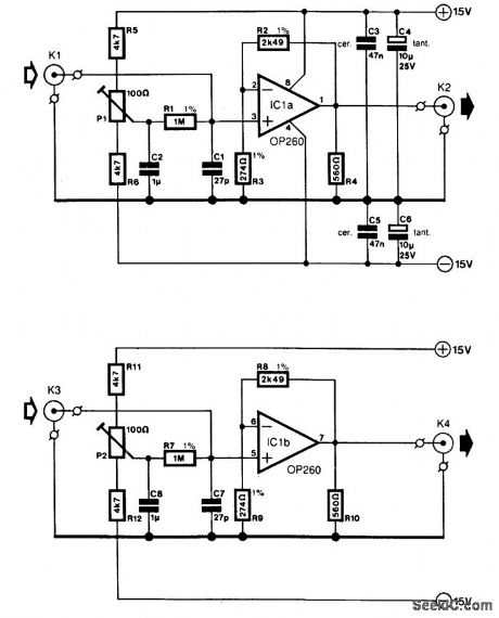
In many oscilloscopes, The most sensitive range is 2 to 5 mV, although it is often possible to improve this to 1 to 2 mV by a variable gain control. To obtain even better sensitivity, the present prearnplifter, which has an amplification of about 10 (20 dB), might be useful.
Because most oscilloscopes have a bandwidth of 20 MHz or more, the amplifier must, of course, have a slightly wider bandwidth and that is achieved with a Type OP260 op amp. This has a slew rate of 550 V/μs (at an amplification of 10) and a bandwidth of 40 MHz that is virtually independent of the amplification.
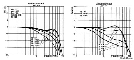
The gain vs. frequency response is not so good, however: as can be seen from Fig. 39-1(b), where the characteristics are given for a number of loads. The hump in the curves depends on the value of the feed-back resistor, whose optimum value appears to be 2.5 kΩ.
The curves in Fig. 39-1(c) accord with different values of R2/R8 for an amplification factor of 10. Some experimentation with the value of R2/R8 for different amplification factors can be instructive. Remember, however, that the output impedance increases from 20 to 225Ω over the frequency range of 10 MHz to 60-70 MHz. It is therefore important to keep all connections on the prototyping board as short as possible and to connect all earth points to a common ground via a separate, heavy track. Also, do not use an IC socket.
An input impedance of 1 MΩ was chosen, which results in a fairly high level of noise at the output (with open-circuit input). This value can be reduced, because otherwise the use of a 1:10 probe will be inhibited; it would give constant problems with the noise. However, when the amplifier is connected to a suitable source, the noise reduction is normally more than ample to obtain a good trace on the screen.Presets Pl and P2 provide compensation for the dc offset and input offset, caused by R1 and R7 respec-tively.
The input bias current for the noninverting input is about 10 times lower than that for the inverting input, which makes the OP260 more suitable for noninverting circuits. The inverting circuit can also give problems because of the low values of R2(R8) and R3 (R9). The input bias current is typically 0.2μA, and the input offset is about 3 mV (max. 7 mV).
In this type of circuit, it is important to use a well-regulated power supply. The power-supply suppres-sion up to 10 kHz is roughly 70 dB, and this reduces with increasing frequency. Any noise or tiny ripple on the supply lines would make the application of the circuit as a small-signal amplifier impossible.
The circuit draws a current of about 14 mA. The slew rate, as with most op amps, is asymmetric and might lead to visible distortion of the signal when the drive to the 560-Ω resistor is high at the higher fre-quencies. (View)
View full Circuit Diagram | Comments | Reading(1502)
V_F_converter_with_20_kHz_full_scale_output_offset_to_improve_dynamic_response
Published:2009/7/20 4:23:00 Author:Jessie
V/F converter with 20 kHz full scale output offset to improve dynamic response (courtesy Analog Devices, Inc.). (View)
View full Circuit Diagram | Comments | Reading(829)
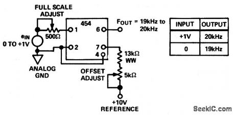
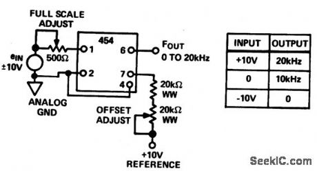
V_F_converter_using_a_flip-flop_to_obtain_a_square_wave_output
Published:2009/7/20 4:22:00 Author:Jessie
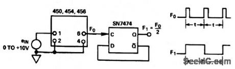
V/F converter using a flip-flop to obtain a square wave output.The full scale output for the 450 and 456 is 10 kHz and 20 kHz for the 454(courtesy Analog Devices, Inc.). (View)
View full Circuit Diagram | Comments | Reading(828)
PROXIMITY_SWITCH
Published:2009/7/9 21:29:00 Author:May
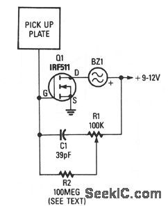
A 3- x -3-inch piece of circuit board, or similar size metal object which functions as the pick-up sensor, is connected to the gate of Q1. A 100-MΩ resistor, R2, isolates Q1's gate from R1, allowing the input impedance to remain very high. If a 100-MΩ resistor cannot be located, just tie five 22-MΩ resistors in series and use that combination for R2. In fact, R2 can be made even higher in value for added sensitivity.Potentiometer R1 is adjusted to where the piezo buzzer just begins to sound off and then carefully backs off to where the sound ceases. Experimenting with the setting of R1 will help in obtaining the best sensitivity adjustment for the circuit.Resistor R1 can be set to where the pick-up must be contacted to set off the alarm sounder. A relay or other current-hungry component can take the place of the piezo sounder to control most any extemal circuit. (View)
View full Circuit Diagram | Comments | Reading(0)
WIEN_BRIDGE_OSCILLATOR_CIRCUIT
Published:2009/7/20 4:22:00 Author:Jessie
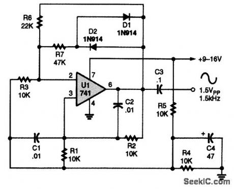
A 741 op amp is connected to a Wien-bridge, audio-sine-wave oscillator configuration, with C1, C2, R1, and R2 determining the circuit's operating frequency. With the use of NPO capacitors and metal-film resistors, the oscillator's frequency is stable enough for use in tone-control applications. The fixed-frequency oscillator shown can easily be converted into a tunable oscillator by substituting a dual-gang linear potentiometer for R1 and R2. Different frequency ranges can be covered by using other matched values for C1 and C2. Larger values produce lower frequencies, and vice versa for small values. (View)
View full Circuit Diagram | Comments | Reading(0)
UHF_MOVEMENT_DETECTOR
Published:2009/7/9 21:26:00 Author:May


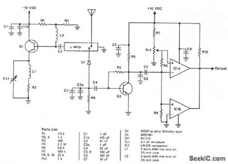
The oscillator is a standard UHF design which delivers about 10 mW at 1.2 GHz. R1 and R2 bias the base of Q1 to 1.2 V via L2. Collector current is set by R3 to about 30 mA. C2 couples the base of Q1 to the stripline circuit. Tuning is provided by CV1, and C1 plus C1a decouple the collector. R2 and R3 are not decoupled, since this could cause instability.Q2 is a simple one-transistor amplifier. C4 and C7 reduce gain below 1.5 and above 100 Hz; the remaining band of frequencies is amplified and passed on to the level detector. Two comparators of IC1 provide level detection. The trigger voltage is set by R7, Rv1, R8, and R9; it is adjustable from 8 to 60 mV by Rv1.Positive voltage swings above the trigger level cause the IC1a output to become low, while negative swings cause IC1b to become low. C8 decouples IC1 from the power supply, and R10 is a pull-up resistor for the open collector output of IC1.
(View)
View full Circuit Diagram | Comments | Reading(1185)
INDUCTANCE_BRIDGE
Published:2009/7/9 21:25:00 Author:May
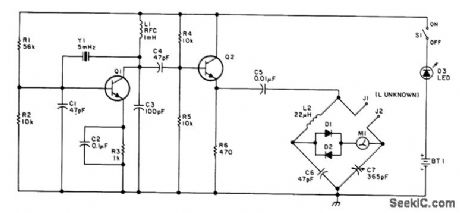
This bridge will measure inductances from about 1 to 30 μH at a test frequency of 5 mHz. A 365-pF AM-type tuning capacitor is used as a variable element. The circuit should be constructed in a metal enclo-sure. Calibration can be done on known inductors or by plotting a curve of the capacitance of the 365-pF capacitor versus rotation and calculating the inductance from this. The range of measurement can be charged by using a different frequency crystal and/or variation of L2 and C6. (View)
View full Circuit Diagram | Comments | Reading(878)
50_watt_PMS_hi_fi_amplifier_for_an_8_ohm_load
Published:2009/7/20 4:22:00 Author:Jessie
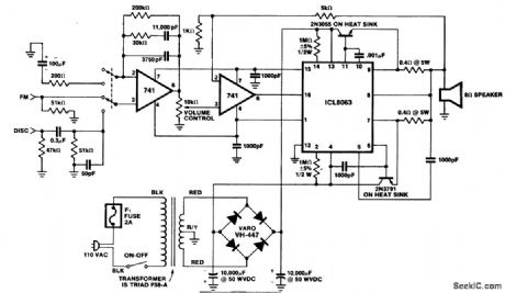
50-watt PMS hi-fi amplifier for an 8-ohm load. This circuit delivers about 56 volts peak to peak across an 8-ohm load. Distortion is about 1 % at 20 kHz. The ganged switch at the input is for selecting either disc or FM radio. The input 741 stage is a preamplifier with RIAA equalization for records (courtesy Intersil, Inc.). (View)
View full Circuit Diagram | Comments | Reading(997)
CAPACITIVE_SENSOR_ALARM
Published:2009/7/9 21:24:00 Author:May
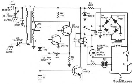


The unit is constructed around a balanced-bridge circuit, using both capacitance and inductance. The bridge consists of capacitors C2 and C3, and the center-tapped winding of T1. One end of the bridge is coupled to ground by C4, while capacitance changes are introduced through C1. A small capacitance change unbalances the bridge and produces an ac signal at the base of Q1. Transistors Q1 and Q2 are connected to form a modifted-Darlington amplifier. The collector load for Q2 is a separate winding of T1 that is connected out-of-phase with the incoming ac signal. That produces a large, distorted signal each time the bridge is unbalanced.The distorted signal is taken from the bridge circuit by a third winding of transformer T1. That signal is then rectified by D6 and applied as a dc signal to the base of Q3. The applied signal energizes the relay, K1, as soon as the unbalanced condition occurs, and the relay drops out as soon as the circuit balance is restored. Of course, for normal alarm use, the relay should be made self-latching, so that the alarm condition remains in effect until the system is reset.An audible alarm, such as a bell or klaxon horn, can be operated from the relay. If a silent alarm is needed, a light bulb can be used. Transformer T1 can be purchased as part #6182 from: Pulse Engineering, P.O. Box 12235, San Diego, CA 92112. (View)
View full Circuit Diagram | Comments | Reading(1193)
V_F_converter_offset_for_bipolar_operation_
Published:2009/7/20 4:21:00 Author:Jessie
V/F converter offset for bipolar operation (courtesy Analog Devices, Inc.). (View)
View full Circuit Diagram | Comments | Reading(775)
BRIDGE_CIRCUIT_WITH_ONE_POWER_SUPPLY
Published:2009/7/9 21:22:00 Author:May
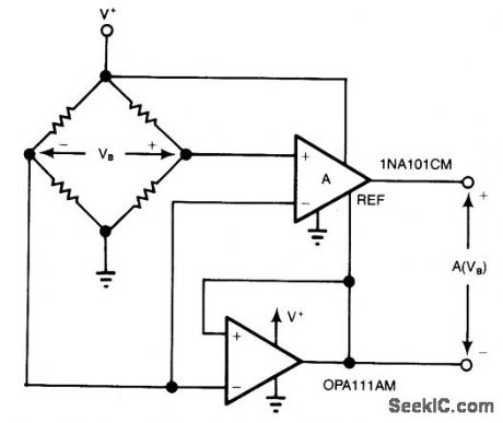
For systems with only one power supply, two op amps act as instrumentation and buffer amps. The OPA111AM buffers the reference mode of the bridge and applies that voltage to the instrumentation amps REF terminal. Output is taken between the amplifier outputs to exclude the fixed output offset.
The additional op amp creates a bridge error of IB x R/2, where IB = bias current of op amp and fi is the resistance of one leg of the bridge. (View)
View full Circuit Diagram | Comments | Reading(720)
LOW_RIPPLE_AT_LOW_COST
Published:2009/7/20 4:21:00 Author:Jessie
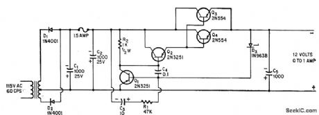
Ripple at output is used to control d-c resistance of series regulator transistors Q3-Q4, to keep ripple below 10 my rms over wide temperature range. Cost is under $15.-R. E. Risely, Power Supply Reduces Ripple by Varying Series Resistance, Electronics, 39:2, p 74-75. (View)
View full Circuit Diagram | Comments | Reading(638)
FAST_OVERVOLTAGE_PROTECTOR
Published:2009/7/9 21:21:00 Author:May
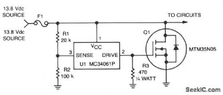


This circuit protects expensive portable equipment against all types of improper hookups and environmental hazards that could cause an overvoltage condition. It operates very quickly and does not latchup, that is, it recovers when the overvoltage condition is removed. In contrast, SCR overvoltage circuits can latch and do not recover, unless the power is removed.Here, U1 senses an overvoltage condition when the drop across R1 exceeds 2.5 V. This causes U1 to apply a positive signal to the gate of Q1, turning it on and shorting the line going to the external circuits. Fuse 1 opens if the transient condition lasts long enough to exceed the i2t rating. (View)
View full Circuit Diagram | Comments | Reading(1137)
12_bit_successive_approximation_A_D_converter_for_bipolar__10_volt_to__10_volt_input_range_with_buffer_followerThe_A_D_chip_is_the_AD572
Published:2009/7/20 4:21:00 Author:Jessie
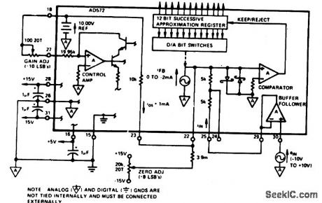
12-bit successive approximation A/D converter for bipolar -10 volt to+10 volt input range with buffer follower,The A/D chip is the AD572(courtesy Analog Devices, Inc.). (View)
View full Circuit Diagram | Comments | Reading(897)
AIR_FLOW_SENSING_THERMISTOR_BRIDGE
Published:2009/7/9 21:20:00 Author:May
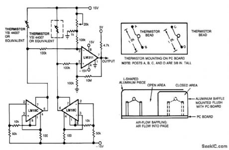
Using the thermistor-bridge circuit, you can detect system-cooling air losses caused by filter or inlet blockage or fan failure. One thermistor is mounted directly in the air flow; the other is baffled. The exposed thermistor senges the temperature in the cooling system; the baffled thermistor senses the ambient temperature in still air. As long as the thermistors are at different temperatures, the bridge stays unbalanced and the circuit produces a logical high, indicating that the cooling system is working. If the air flow stops, the exposed thermistor will reach ambient temperature, the bridge will become balanced, and the circuit will indicate ventilation-system failure by producing a logical low.
The bridge circuit's matched thermistors are biased 'oy matched-current sources. Two LM10C operational, amplifiers act as constant-current sources, and an LM311 comparator senses the difference between the voltage drops across the thermistors, producing the logical high when the bridge is unbal-anced and the logical low when the bridge is balanced. Use a 20-kΩ potentiometer to set the comparator's threshold; this setting determines the minimum air flow that will cause the circuit to produce a logical high. (View)
View full Circuit Diagram | Comments | Reading(1877)
| Pages:878/2234 At 20861862863864865866867868869870871872873874875876877878879880Under 20 |
Circuit Categories
power supply circuit
Amplifier Circuit
Basic Circuit
LED and Light Circuit
Sensor Circuit
Signal Processing
Electrical Equipment Circuit
Control Circuit
Remote Control Circuit
A/D-D/A Converter Circuit
Audio Circuit
Measuring and Test Circuit
Communication Circuit
Computer-Related Circuit
555 Circuit
Automotive Circuit
Repairing Circuit