Amplifier Circuit
RF_WIDEBAND_ADJUSTABLE_AGC_AMPLIFIER
Published:2009/7/9 22:58:00 Author:May | From:SeekIC

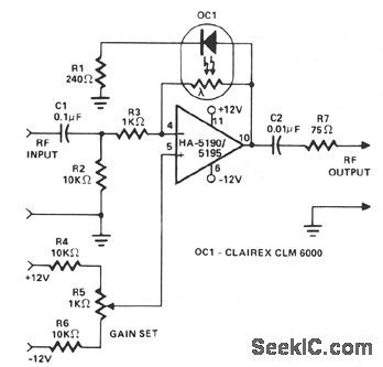
This circuit functions as a wideband adjustable AGC amplifier.With an effective bandwidth of approximately 10 MHz,it is capable of handling rfinput signal frequencies from 3.2 to 10 MHz at levels ranging from 40 mV up to 3 V pk-pk.AGC action is achieved by using optocoupler/isolater OC1 as part of the gain control-feedback loop.In operation, the positive peaks of the amplifed output signal drive the OC1 LED into a conducting state. Since the resistance of the OC1 photosensitive element is inversely proportional to light intensity, the higher the signal level, the lower the feedback resistance to the op amp inverting input. The greater negative feedback lowers stage gain. Any changes in gain occur smoothly because the inherent memory characteristic of the photoresistor acts to integrate the peak signal inputs. In practice, the stage gain is adjusted automatically to where the output signal positive peaks are approximately one diode drop above ground.Gain set control R5 applies a fixed dc bias to the op amp noninverting input, thus establishing the steady state-zero input signal current through the OC1 LED and determining the signal level at which AGC action begins.The effective AGO range depends on a number of factors, including individual device characteristics, the nature of the rf drive signal, the initial setting for R5, et al. Theoretically, the AGC range can be as high as 4000:1 for a perfect op amp because the OC1 photoresistor can vary in value from 1 MΩ with the LED dark to 250 Ω with the LED fully on.
Reprinted Url Of This Article:
http://www.seekic.com/circuit_diagram/Amplifier_Circuit/RF_WIDEBAND_ADJUSTABLE_AGC_AMPLIFIER.html
Print this Page | Comments | Reading(3)

Article Categories
power supply circuit
Amplifier Circuit
Basic Circuit
LED and Light Circuit
Sensor Circuit
Signal Processing
Electrical Equipment Circuit
Control Circuit
Remote Control Circuit
A/D-D/A Converter Circuit
Audio Circuit
Measuring and Test Circuit
Communication Circuit
Computer-Related Circuit
555 Circuit
Automotive Circuit
Repairing Circuit
Code: