
Circuit Diagram
Index 763
GLITCH_FREE_CLIPPER
Published:2009/7/12 20:57:00 Author:May
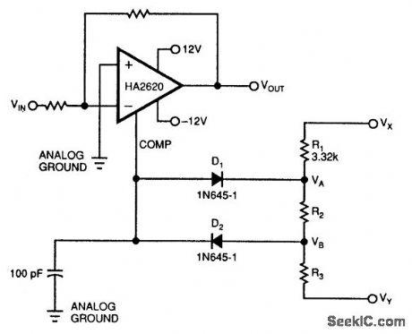

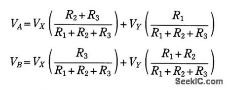
Adding a simple clamping circuit to a Harris 2620 high-speed op amp produces a glitch-free amplifier/ clipper. The op amp pin that controls the device's bandwidth is a high-impedance, isolated input. This pin also tracks the device's output voltage.Therefore, D1, D2, R1, R2, and R3 will clamp the amplifier's output voltage only when the amplifier's input voltage exceeds your clamping-voltage limits. VD is the diode drop of D1 or D2. The two clamp voltages, VA+VD and VB-VD, are:where VX and VY are the clamping circuit's bias voltages. Choosing R1 lets you determine the values of R2 and R3. Try a value for R1 around 3 kΩ.One example of this circuit had clamping voltages of ±3.7 V and exhibited THD below -75 dB for a sinusoidal, 30-kHz input signal. When the input signal increased beyond the ±3.7-V clamping voltage, the clipper symmetrically clamped the output voltage with no glitches in the waveform. (View)
View full Circuit Diagram | Comments | Reading(717)
INHIBIT_DRIVER
Published:2009/7/12 20:56:00 Author:May

Used in coincident-current digital data buffer memory.-D. Haagens, Compact Memories Have Flexible Capacities, Electronics, 32:40, p50-53. (View)
View full Circuit Diagram | Comments | Reading(551)
MATRIX_READOUT
Published:2009/7/12 20:54:00 Author:May
Used for data reduction in telephone traffic data recorder system to permit recording all information on a call as one entry. Coincidence circuit Q1-Q2 provides reliable sensing of matrix output in presence of noise generated by rotary switches and relays.-J. W. Blonchard, E. C. Bellee, and J. Smith, Ferrite Memories Simplify Telephone Data Analysis, Electronics, 32:41, p 68-70. (View)
View full Circuit Diagram | Comments | Reading(516)
VOLTAGE_COMPARATOR
Published:2009/7/12 20:54:00 Author:May
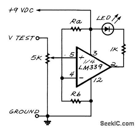
The LED turns on when the input voltage at pin 5 of the LM339 falls below the reference voltage at pin 4. (View)
View full Circuit Diagram | Comments | Reading(0)
FAST_TTL_COMPATIBLE_COMPARATOR
Published:2009/7/12 20:53:00 Author:May
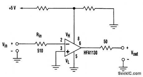
The HFA1130 by Harris Semiconductor is useful as a comparator. Depicted is an inverting 2-ns comparator with TTL-compatible output levels that are realized by using the HFA1130 output-limiting, current-feedback amplifier. (View)
View full Circuit Diagram | Comments | Reading(701)
10_h_FET
Published:2009/7/12 20:53:00 Author:May
Long duration timer gives adjustable delays up to 10 hours before turning Q3 on to give output voltage.-Circuits, 73 Magazine, Feb. 1974, p 101. (View)
View full Circuit Diagram | Comments | Reading(551)
MEMORY_STROBING_PULSE_GATE
Published:2009/7/12 20:53:00 Author:May


Used in generating precisely defined strobes for coincident-current memory. Uses drive-sampling core instead of clock signal to produce strobe at time when signal-to-noise ratio is highest.-A. H. Ashley and E. U. Cohler, Solving Noise Problems in Digitctl Computer Memories, Electronics, 33:13, p72-74. (View)
View full Circuit Diagram | Comments | Reading(513)
ADJUSTABLE_COMPARATOR
Published:2009/7/12 20:52:00 Author:May

The setting of potentiometer R2 determines the level at which this comparator circuit will switch. The output can be used to drive any device needing a comparator signal, within the drive capabilities of the particular op amp used (741 is shown). (View)
View full Circuit Diagram | Comments | Reading(3467)
FOUR_LEVEL_VOLTAGE_COMPARATOR
Published:2009/7/12 20:52:00 Author:May
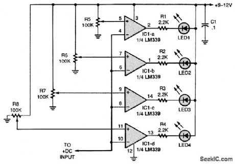
This four-level voltage detector can be used as a bar-graph voltmeter. Simply set each potentiometer (R5 to R8) for a specific voltage. (View)
View full Circuit Diagram | Comments | Reading(3425)
10_min_DELAY
Published:2009/7/12 20:52:00 Author:May
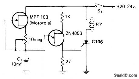
MPF103 JFET makes charging current of C1 constant regardless of degree of charge, to give longer charging time and longer timedelay. After delay determined by setting of 10-megohm pot, UJT conducts and discharges Q, through 27-ohm resistor, triggering SCR and energizing relay. Open S1 to reset circuit.-I. Math, Math's Notes, CQ, April 1974, p 64-65 and 91-92. (View)
View full Circuit Diagram | Comments | Reading(727)
VOLTAGE_WINDOW_COMPARATOR
Published:2009/7/12 20:51:00 Author:May

This window comparator determines if a voltage is between two limits, upper and lower.Using a digital voltmeter, set the reference voltages in this voltage window to the same values.Then vary one to set the width of the window; when the input voltage is within the window area, LED1 will light. (View)
View full Circuit Diagram | Comments | Reading(0)
APPLIANCE_TIMER
Published:2009/7/12 20:50:00 Author:May
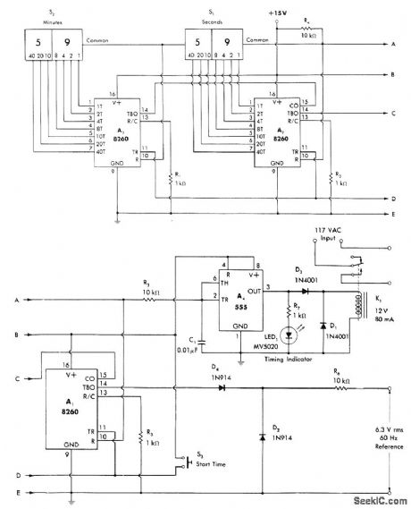
Controls intervals up to 1 h in 1-s increments as programmed by thumb wheel switches S1 and S2. Circuit is basically two-stage programmed counter driven by 1-s clock derived from 60-Hz power line. A1 is connected as divide-by-60 counter triggered by 60-Hz signal developed across D2. 1-Hz output from A1 triggers A2 which in tum triggers A3, all programmable timers. When S3 is closed, R4 bus goes low to start timing cycle. Relay driver A4 holds relay K1 closed for application of AC power to device being controlled and energizing of LED to indicate active timing cycle. Applications include uses as kitchen and darkroom timers,-W. G. Jung, IC Timer Cookbook, Howard W. Sams, Indianapolis, IN, 1977, p 214-218. (View)
View full Circuit Diagram | Comments | Reading(1893)
DUAL_VOLTAGE_COMPARATOR
Published:2009/7/12 20:50:00 Author:May
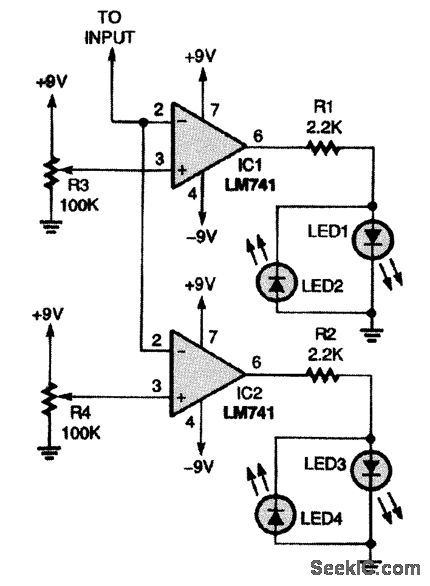
Use this dual comparator to monitor a battery while it's charging; the circuit will let you check for under- and overvoltage conditions.R3 and R4 set the trip levels at which the LEDs are activated. Almost any standard LEDs can be used. LED current is about 3 to 4 mA, as determined by the op-amp capability and resistors R1 and R2. (View)
View full Circuit Diagram | Comments | Reading(2086)
CODE_PRACTICE_OSCILLATOR
Published:2009/7/12 20:49:00 Author:May

This versatile code-practice oscillator has a variable frequency and volume control. The unit is especially suitable for use by small groups that are interested in learning and practicing code. A single 4049 CMOS hex inverting buffer is the heart of the oscillator, with inverters U1-a and U1-b making up the variable audio-oscillator circuit. The oscillator's output is coupled to the speaker-driver circuit through the CW (Morse code) key S1. The audio frequency of the oscillator (hence, its tone) is varied by the potentiometer. R3 is used to vary the speaker's volume. (View)
View full Circuit Diagram | Comments | Reading(0)
INFRARED_CODE_PRACTICE_RECEIVER
Published:2009/7/12 20:47:00 Author:May
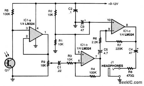
An IR phototransistor, Q1, is directly-coupled to the input of op amp IC1-a. The output of IC1-a is fed through the gain-control potentiometer R9 to the input of op amp IC1-b, which has a voltage gain of 10. Section IC1-b's output drives IC1-c, which has a voltage gain of 100. The output of IC1-c supplies audio to the heddphones via J1. The IR phototransistor can be mounted in reflectors to increase the CPO's operating range. (View)
View full Circuit Diagram | Comments | Reading(1613)
REPEAT_CYCLE
Published:2009/7/12 20:47:00 Author:May
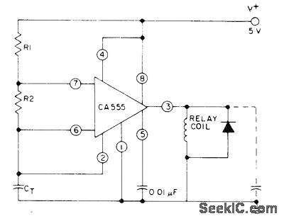
RCA CA555 is connected for astable operation in which total period is sum of individual perids t1 and t2, where t1 = 0.693(R1 + R2)CT and t2 = 0.693R2CT. With 5-V supply, output voltage has rectangular pulses with interval t1 separated by interval t2. With optional capacitor connected, voltage across capacitor is sawtooth that rises for interval t1 and decays for interval t2.- Linear Integrated Circuits and MOS/ FET's, RCA Solid State Division, Somerville, NJ, 1977, p 56. (View)
View full Circuit Diagram | Comments | Reading(693)
INFRARED_CODE_PRACTICE_TRANSMITTER
Published:2009/7/12 20:46:00 Author:May

A 555 timer, IC1, is connected in an audio-oscillator circuit with its frequency set by potentiometer R6. Transistor Q1, with the CW key up, is biased on, thereby holding pin 5 of IC1 low and keeping it turned off. The 555 timer's output, at pin 3, ties to the gate of a power hexFET, Q2, which drives the three IR emitters, LED1 to LED3. Placing the CW key in the down position turns the 555 oscillator on. That sends out the audio tone signal via IR. (View)
View full Circuit Diagram | Comments | Reading(1256)
WIRELESS_FM_CODE_PRACTICE_TRANSMITTER
Published:2009/7/12 20:45:00 Author:May

The circuit shown is a low-power, tone-modulated FM transmitter that can be used with any FM broadcast receiver for code practice. Transistor Q1 and its associated components make up a phaseshift audio-frequency generator circuit. Potentiometer R11 sets the tone frequency. Transistor Q2 is connected in a high-frequency RE oscillator circuit that operates in the FM broadcast band. Potentiometer R12 sets the modulation level. Transistor Q3 operates as a switch, turning on the FM transmitter each time the CW key is closed. Coil L1 is a homemade air-wound coil. Take a 6 1/2-in length of 20-gauge enamel-covered wire and close-wind it around a 1/4-in-diameter form; leave about 1/4 in free at each end. Remove the insulation from the ends and slide the coil off the form. The overall length of the finished coil should be about 1/4 in. Set R11 and R12 to midposition and close the CW key. Then set your FM receiver to a clear spot on the low end of the dial and slowly adjust C8. Once the tone is heard, R11 can be set for the desired tone frequency and the tone level set by R12. If your oscillator won't tune to the top end of the band, carefully stretch the windings of L1 and retune. The circuit's operating range can be increased by adding a very short antenna to the emitter of Q2. (View)
View full Circuit Diagram | Comments | Reading(2455)
RAMP_GENERATOR_DRIVES_TRlGGER
Published:2009/7/19 21:39:00 Author:Jessie

Circuit is relaxation oscillator providing short, fast pulses for triggering mvbr. Upper operating frequency is about 1 Mc for values shown. Efficiency is high yet total component cost is under $2.-C. F. Andren, High Efficiency Relaxation Oscillator, EEE, 14:4, p 43. (View)
View full Circuit Diagram | Comments | Reading(828)
Fast_settling_op_amp_with_gain_of__1
Published:2009/7/19 21:30:00 Author:Jessie
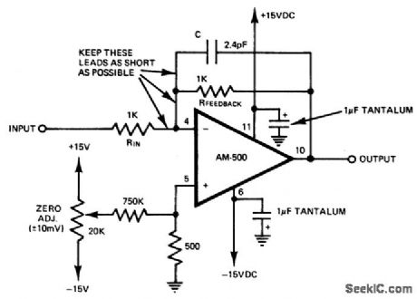
Fast-settling op amp with gain of -1. For gains larger than -1 use an input resistor valued at 500 ohms or less and pick a feedback resistor for the required gain, i.e., 1K for -2, 1.5K for -3, etc. (courtesy Datel Systems, Inc.). (View)
View full Circuit Diagram | Comments | Reading(808)
| Pages:763/2234 At 20761762763764765766767768769770771772773774775776777778779780Under 20 |
Circuit Categories
power supply circuit
Amplifier Circuit
Basic Circuit
LED and Light Circuit
Sensor Circuit
Signal Processing
Electrical Equipment Circuit
Control Circuit
Remote Control Circuit
A/D-D/A Converter Circuit
Audio Circuit
Measuring and Test Circuit
Communication Circuit
Computer-Related Circuit
555 Circuit
Automotive Circuit
Repairing Circuit