
Circuit Diagram
Index 771
PRACTICE_OSCILLATOR
Published:2009/7/11 5:04:00 Author:May


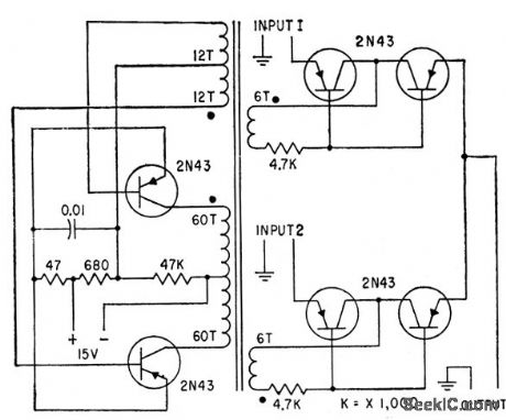
Simple design provides for adjustment of both volume and tone.-Circuits, 73 Magazine, July 1974, p 81. (View)
View full Circuit Diagram | Comments | Reading(794)
CODE_PRACTICE
Published:2009/7/11 5:03:00 Author:May
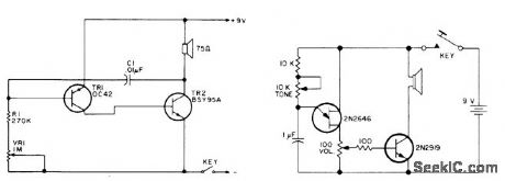
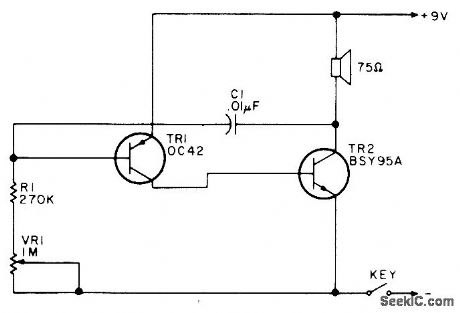
Simple AF oscillator drives loudspeaker for producing audio tone when key in negative supply lead is closed. Adjust VR1 for most pleasing tone.-Circuits, 73 Magazine, July 1975, p 154. (View)
View full Circuit Diagram | Comments | Reading(704)
VLF_CONVERTER
Published:2009/7/11 5:03:00 Author:May
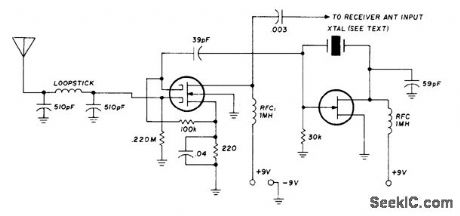
Uses low-pass filter instead of usual tuned circuit, so only associated receiver need be tuned. Measured threshold sensitivity is about 20 μv. Transistors used in dual-gate MOSFET mixer and FET oscillator are not critical. Crystal can be any frequency compatible with tuning range of receiver used. With 3.5-MHz crystal, 3.5 MHz on receiver dial corresponds to 0 kHz and 3.6 MHz to 100 kHz.-R. N. Coan, VLF Converter, Ham Radio, July 1976, p69. (View)
View full Circuit Diagram | Comments | Reading(0)
220_MHz_TO_28_MHz
Published:2009/7/11 5:00:00 Author:May
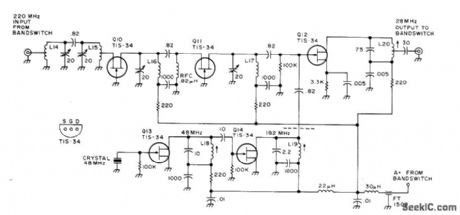
Contains bandpass filter, grounded-grid RF amplifier stages Q10-Q11, mixer Q12, and crystal oscillator Q13-Q14. Developed for use in all-band double-conversion superheterodyne receiver for AM narrow-band FM, CW, and SSB operation. Supply is 13.6 V regulated. Article gives all circuits of receiver. -D. M. Eisenberg, Build This All-Band VHF Receiver, 73 Magazine, Jan. 1975, p 105-112. (View)
View full Circuit Diagram | Comments | Reading(2184)
LASER_POWER_SUPPLY
Published:2009/7/11 5:00:00 Author:May

IC1 is a 555 timer running at about 16 kHz. This IC drives Q1, a TIP146, which produces a 12-V square wave across T1 primary. This produces between 800 and 2,000 V across the secondary, which is doubled to 3 to 5 kV. When the load (laser) on the power supply increases, current Q2 is turned on, which energizes RY1. This changes the duty cycle of the 555 timer. To adjust this supply, set R12 and R13 at the center. Adjust R12 until the laser tube triggers, and make sure that the relay pulls in. If the relay chatters, adjust R12. If the full-clockwise adjustment of R12 fails to ignite the tube, adjust R13. (View)
View full Circuit Diagram | Comments | Reading(0)
PULSE_COINCIDENCE_DETECTOR
Published:2009/7/11 4:59:00 Author:May

Detecls coincidences between pulses of random length and spacing occurring in two separctte channels, to permit counting only pulses that do not overlap.-K. R. Whittington and G. Robson, Novel Anticoincidence Circuit Detects Pulse overlap, Electronics, 35:26, p82. (View)
View full Circuit Diagram | Comments | Reading(0)
144_MHz_T0_28_MHz
Published:2009/7/11 4:58:00 Author:May

144 MHz T0 28 MHz-Contains bandpass filter, grounded-grid RF amplifier stages Q5- Q6, mixer Q7, and crystal oscillator Q8-Q9. Developed for use in all-band double- conversion superheterodyne receiver for AM, narrow-band FM, CW, and SSB operation. Supply is 13.6 V regulated. Article gives all circuits of receiver-D. M. Eisen. berg, Build This All-Band VHF Receiver, 73 Magazine, Jan. 1975, p 105-112. (View)
View full Circuit Diagram | Comments | Reading(3478)
KEYER_WITH_MEMORY_2
Published:2009/7/11 4:57:00 Author:May
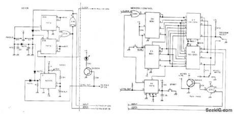
Clock Z1 is NE555 timergiving keying speed range of 5 to 35 WPM.Flip-flops Z2A and Z2B count clock pulses to provide self-completing dits and dahs with spaces. Z4 and Z5 are 4-bit binary counters used for addressing static 256 × 1 bit RAM. To program keyer, switch to write, hit START button, and feed in message on keyer paddle. To send message back, switch to read and hit START again. To clear address counter if error is made, or for changing message, hit RESET switch and start over again.-D. W. Sewhuk, Contest Special Kever, 73 Magazine, Feb. 1977, p 38. (View)
View full Circuit Diagram | Comments | Reading(571)
50_MHz_TO_28_MHz
Published:2009/7/11 4:57:00 Author:May
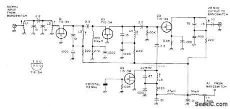
Contains bandpass filter, two grounded-grid RF amplifier stages Q1-Q2, mixer Q3, and crystal oscillator Q4. Developed for use in all-band double-conversion superheterodyne receiver for AM narrow-band FM, CW, and SSB operation. Supply is 13.6 V regulated, Article gives all circuits of receiver, -D. M. Eisenberg,Build This All-Band VHF ReceiVer,73 Magazine,Jan,1975,p 105-112. (View)
View full Circuit Diagram | Comments | Reading(1512)
SIMPLE_KEYER
Published:2009/7/11 4:56:00 Author:May

Based on rapid charging of capacitors and controlled discharge through relay coil. When C, has discharged to relay release voltage, relay drops out and cycle starts over again as long as dot side of paddle is pressed. Dashes are similarly formed by C1. R4 adjusts speed from 10 to 40 WPM. K1 is DPDT plate-current relay having 1K to 10K resistance.-J. J. Russo, An Inexpensive Electronic Keyer, CQ, Aug. 1971, p 58. (View)
View full Circuit Diagram | Comments | Reading(839)
1_3_DOT_DASH_KEYER
Published:2009/7/11 4:55:00 Author:May
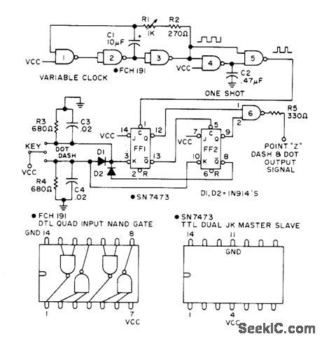
Gives accurate 1 :3 dotdash ratio at any desired keying speed, with self-completing characters. NAND gates 1, 2, and 3 of first FCH191 form variable-frequency square-wave oscillator, with C1, R1, and R2 determining frequency. With values shown, frequency is adjustable from about 150 to 1500 Hz, equivalent to code speed range of about 4 to 40 WPM. NAND gates 4 and 5 form mono MVBR. Flip-flops FF1 and FF2 are SN7473 TTL JK master-slave, acting with D1, D2, and NAND gate 6 to generate dots and dashes.-H. P. Fischer, Versatile IC Keyer, 73 Magazine, Sept. 1973, p 69-71. (View)
View full Circuit Diagram | Comments | Reading(820)
COCKCROFT_WALTON_CASCADED_VOLTAGE_DOUBLER
Published:2009/7/11 4:55:00 Author:May
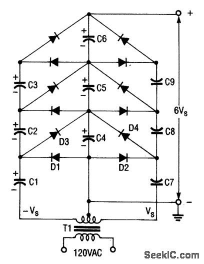
A center-tapped transformer of secondaryvoltage.Two VS can be used to power a voltage multiplier. For higher voltages,simply add more sections. (View)
View full Circuit Diagram | Comments | Reading(1017)
20_KC_CHOPPER
Published:2009/7/11 4:54:00 Author:May
Square-loop-core oscilkttor drives chopper at up to 20 kc for continuously monitoring two d-c voltages.-J. W.Higginbotham And H. H. Douglass, Voltage Compctrator with High-Speed Switches, Electronics, 32:5, p56-58. (View)
View full Circuit Diagram | Comments | Reading(554)
VOLTAGE_DOUBLERS
Published:2009/7/11 4:52:00 Author:May
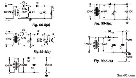
During the first half-cycle (Fig. 99-5(a)), D1 conducts, D2 cuts off, C1 charges to 170 V peak, and C2 discharges through RL For the second half-cycle (Fig. 99-5(b)), the input polarity is reversed, and both the input and C1 are in series, which produces 340 V (peak). Now, D1 cuts off, while D2 conducts, and the current divides between C2 and RL; the cycle then repeats. Two Half-Wave Rectifiers, one with a positive output (Fig. 99-5(c)) and one negative (Fig. 99-5(d)), combine to make a full-wave voltage doubler (Fig. 99-5(e)). (View)
View full Circuit Diagram | Comments | Reading(684)
CONTROL_AMPLIFIER
Published:2009/7/11 4:50:00 Author:May

Converts output of 20-kc chopper to d-c error signal.Amplifier output is rectified by diodes rather than demodulated,since polarity of error is of no concern.-J.W.Higginbotham and H.H.Douglass.Voltage Comparator with High-Speed Switches,Electronics.32:5,p56-58 (View)
View full Circuit Diagram | Comments | Reading(489)
HIGH_VOLTAGE_NEGATIVE_ION_GENERATOR
Published:2009/7/11 4:49:00 Author:May

A modified B/W TV flyback transformer is used in this circuit with a voltage multiplier to produce 9- to 14-kV negative voltage. This is connected to a discharge needle to produce negative ions. (View)
View full Circuit Diagram | Comments | Reading(4563)
10_000_Vdc_SUPPLY
Published:2009/7/11 4:45:00 Author:May

A CMOS oscillator (U1A) drives. U1B through U1F, which drives Q1, which generates a 12-Vpp square wave across the primary of T1. This square wave is applied to a rectifier-multiplier circuit consisting of D1 through D10 (each is two 1N4007 diodes in series) and C3 through C12. About 10 kV is available. (View)
View full Circuit Diagram | Comments | Reading(688)
TWO_STAGE_SWITCH
Published:2009/7/11 4:43:00 Author:May

D-c output from carrier amplifer triggers switch consisting of two-stage complementary-coupled nonlinear am pliler, with zener diode in series with input to minimize drift, when difference between two d-c voltages exceeds preset threshold voltages of as little as 100 microvolts for only 300 microsec. Can handle 2 amp. R1 is 100,000 ohms and R2 is 100 ohms.-J. W. Hig-ginbotham and H. H. Douglass, Voltage Comparcttor with High-Speed Switches, Electronics, 32:5, p56--58. (View)
View full Circuit Diagram | Comments | Reading(721)
CORONA_WIND_GENERATOR
Published:2009/7/11 4:42:00 Author:May

This 25-stage voltage doubler will generate corona wind. 120 Vac, or 3.75 kVdc when powered from 240 Vac.or 7.5 kvdc when powered 240 Vac (View)
View full Circuit Diagram | Comments | Reading(1530)
AUTOPILOT_COMPARATOR_ALARM
Published:2009/7/11 4:39:00 Author:May


Actives alarm or disengages autopilot when signals from dual accelerometers differ apperciably.indicating malfunction.-C. W. McWilliams, Designing Safety Into Automotic Pilot Sys-tems, Electronics, 31:45, p69-71. (View)
View full Circuit Diagram | Comments | Reading(629)
| Pages:771/2234 At 20761762763764765766767768769770771772773774775776777778779780Under 20 |
Circuit Categories
power supply circuit
Amplifier Circuit
Basic Circuit
LED and Light Circuit
Sensor Circuit
Signal Processing
Electrical Equipment Circuit
Control Circuit
Remote Control Circuit
A/D-D/A Converter Circuit
Audio Circuit
Measuring and Test Circuit
Communication Circuit
Computer-Related Circuit
555 Circuit
Automotive Circuit
Repairing Circuit