
Circuit Diagram
Index 779
PSEUDORANDOM_DIGITAL_GENERATOR
Published:2009/7/11 3:19:00 Author:May

Uses two Am687 dual sampling comparators toimplement 200-Mb/s pseudorandom digital-sequence generator for checking and measuring performance of high-speed digital communication equipment. Produces sequence length of 127 bits, but delay-line length can be changed to give any desired other sequence length. Circuit acceptsfrom 195to 203 Mb/s,which is more than adequate for systems using crystal clock having ±0.1% frequency variation. Article describes operation and gives timing diagram.-G. L. Meyer, Sampling Comparators-They Sub for High-Speed Logic and Produce Power, Cost and Space Savings, EDN Magazine, Sept. 5,1977, p 71-74. (View)
View full Circuit Diagram | Comments | Reading(766)
5_V_AT_2_A
Published:2009/7/17 2:33:00 Author:Jessie
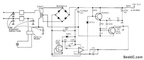
Developed as supply for receiver frequency counter having LED display. FET having IDSS of about 7.5 mA serves in place of 1200-ohm resistor as current regulator. Power transformer is Triad F-26X with secondary rated 12.6 V center-tapped at 2.5 A.-H. H. Cross, The Chintzy 12, 73 Magazine, Feb. 1977, p 40-41. (View)
View full Circuit Diagram | Comments | Reading(701)
SIMPLE_AM_RADIO
Published:2009/7/17 2:33:00 Author:Jessie

An AM radio can be built of a simple diode detector and an audio amplifier. A random length of wire always serves as an antenna. L1 is an adjustable ferrite loopstick of the type used in transistor radios. (View)
View full Circuit Diagram | Comments | Reading(3611)
TRANSISTOR_TESTER
Published:2009/7/11 3:17:00 Author:May

Will test conventional bipolar transistors, JFETs, MOSFETs, Darlingtons and UJTs. Audible note between 1000 and 5000 Hz from connected loudspeaker indicates that device is functioning as amplifier and gives relative indication of gain and noise figure. Most devices can be tested in-circuit. Among similar JFETs or MOSFETs, those producing lowest tone pitch have lowest noise figure. Among similar devices of any type, those producing loudest tone have highest gain. Tester feeds back audio signal through two transformers to create sustained oscillation when amplifying device is connected to proper terminals. S1 applies positive ornegative voltage through audio output transformer T2 to device under test. C3 and C4 must be nonpolarized electrolytics because R1 and R2 may produce either positive or negative voltage depending on device being tested. T1 and T2 have 1200-ohm primary and 8-ohm secondary (Calectro DI-724). Note above 10,000 Hz means device has some gain but does not meet specifications or is connected incorrectly. For MOSFETs, source and substrate are both connected to source terminal.-W. E. Anderson, A Universal Transistor Tester, QST, Dec. 1975, p 26-28. (View)
View full Circuit Diagram | Comments | Reading(0)
UNDERVOLTAGE_DISCONNECT_SWITCH
Published:2009/7/17 2:32:00 Author:Jessie

In an effort to conserve energy, simple shutdown schemes are incorporated into many battery-operated circuits. Not all circuits lend themselves to direct control, however. Instead, the supply must be turned off by a switch. The LTC1477 high-side switch is designed for this purpose and includes short-circuit current limiting and thermal shutdown to guard against faulty loads. The figure shows the LTC1477 and LTC699 conjoined in an undervoltage disconnect application. The LTC699 microprocessor supervisor disables the LTC1477; hence, the load is disabled whenever the input voltage falls below 4.65 V. An external logic signal applied to the gate of Q1 can also disable the LTC1477. When enabled, the LTC1477 output ramps over a period of approximately 1 ms, thereby limiting the peak current in the load capacitor to 500 mA. This prevents glitches on the 5-V source line that might otherwise affect adjacent loads. (View)
View full Circuit Diagram | Comments | Reading(867)
FREQUENCY_SWEEPER
Published:2009/7/11 3:16:00 Author:May

Sawtooth output of UJT varies sinusoidal output frequency of Optical Electronics 3370 voltage-to-frequency transducer, as required for checking frequency response of active and passive networks. R1 determines sweep width. Center frequency of sweep output can be changed by adding voltage to sawtooth or adjusting 3370. Sweep speed can be increased by reducing value of 1-μF tantalum capacitor.- Sweep Generator Using a Voltage-to-Frequency Transducer, Optical Electronics, Tucson, AZ, Application Tip 10059. (View)
View full Circuit Diagram | Comments | Reading(921)
200_BIT_MEMORY
Published:2009/7/11 3:15:00 Author:May

Drawback of volatile codestoring memory is offset by low cost and com parative ease of programming. IC1 is Signetics 2511D MOS dual 200-bit shift register whose digital levels are shifted one position for each dock pulse. Inverters I1 and I2 of CMOS hex inverter IC3 form variable-frequency gated square-wave clock oscillator controlled by state of flip-flop FF2 in 74C74 CM0S dual D flip-flop. Shift register must first be cleared by setting DATA and CONTROL switches to ground and RECIRCULATE switch to hold, then pressing START button (with speed control set fast) until register is full of zeros, Release START button and switch control to +6 V for about 10 s. Now set CONTROL to ground and start programming. To enter dah, switch manual clock through three complete up-center/down-center cycles, switch data line to ground, and cycle manual clock through one cycle to insert space into memory. To enter dit, switch manual clock through only one up/down cycle. Continue until entire message is entered in register, switch to RECIRCULATE, and push START switch. Message will now be sent in perfect code at any desired speed.-B. P. Vandenberg, An Inexpensive Memory Keyerfor Contests, CQ, May 1976, p 50-51. (View)
View full Circuit Diagram | Comments | Reading(624)
SIMPLE_MONOCHROME_TV_PATTERN_GENERATOR
Published:2009/7/11 3:14:00 Author:May

Using a Plessey ZNA234E IC, this generator produces sync, blankin gray bars lines, dots and crosshatch patteflls. (View)
View full Circuit Diagram | Comments | Reading(2063)
PLL_CODE_REGENERATOR
Published:2009/7/11 3:13:00 Author:May

Permits comfortable listening to CW signals deeply embedded in noise, hash, and interference, by detecting one particular CW transmission and keying independent oscillator with its signal. Consists of signal amplifier Q1, narrow-band PLL frequency detector and trigger U1, PLL function generator U2, gate Q2, and AF output amplifier U3. In absence of triggering signal, output pin 8 of U1 presents high impedance to ground. With trig-gering frequency, output presents low impedance to ground. Oscillator U2 is gated by un through Q2.-C. R. Lewartand R. S. Libenschek, CW Regenerator for Interference-Free Communications, Ham Radio, April 1974, p 54-56. (View)
View full Circuit Diagram | Comments | Reading(1072)
RECORDED_CODE_KEYER
Published:2009/7/11 3:12:00 Author:May

CW message recorded on cassette tape with keyed tone generato r is played back for keying transmitter with frequently repeated messages. Transmitted signal is essentially perfect reproduction of recording. Automatic transmission can be stopped at any point by tapping hand key; this deactivates tape recorder for manual keying of transmitter. All transistors are 2N2222 or equivalent BCY58. Use 24-V reed relays with 1K coil resistance. Pilot lamps are 24 V rated up to 3 W.CR1 is silicon diode. Whenever recorder emits beep, positive signal appears at base of Q2, making it conduct and activate K1 whose contacts go to key jack of transmitter.-A. Day, An Audio Tape-Controlled CW Keyer, CQ, Nov. 1971, p 31-32. (View)
View full Circuit Diagram | Comments | Reading(849)
CLOCK_RING_COUNTER
Published:2009/7/11 3:11:00 Author:May

Switthing element is silicon controlled switch that approximates flip-flop, turning on when low-level positive pulse is applied to its base, and remaining on until turned off by negative pulse. Used us memory device to retain registered count until next input pulse makes bit transfer to following stage.-R.S. Reed, Rugged Arming Fuzing Timer for Atomic Artillery Missile, Electronics, 34:38, p48-51. (View)
View full Circuit Diagram | Comments | Reading(760)
SYNC_SEPARATOR
Published:2009/7/11 3:08:00 Author:May

This circuit separates the synch from the composite video signal.It uses a two-transistor comparator.Output is 9 VPP a 0.5-VPP (minimum) video input signal. (View)
View full Circuit Diagram | Comments | Reading(4954)
LED_DISPLAY_FOR_ASCLL_CODE
Published:2009/7/11 3:07:00 Author:May

Shows code for any ASCLL keyboard character as aid in debugging keyboard matrix wiring. Requires only two 7400 quad NAND gates, eight resistors, and eight LEDs. High input to gate forces output low, grounding LED and lighting it. On standby with positive logic, all LEDs are lit with negative logic ,all are dark on stangby .arrange LEDs on keyboard so rightmost LED represents least significantbit (DO)and leftmost LED represents parity bit. Using positive logic, ASCLL code for any depressed key will show as lit LED for 1 and dark LED for o. Pin 14 of 7400 is +5 V, and pin 7 is ground.-B. Brehm. Using a Keyboald ROM, BYTE, May 1977, p 76-.82. (View)
View full Circuit Diagram | Comments | Reading(1509)
PROM_CW_IDENTIFIER
Published:2009/7/11 3:07:00 Author:May

Call letters stored in 8223 PR0M U3 drive 74151 multiplexer/data selector U4 for keying NE555 audio oscillator U5 which feeds transmitter mike input through RA.Timed holdoff keeps identifier from being rekeyed within spedfied time period, with reiden.tifying at end of period. Article covers operation of circuit and gives construction and programming details,ID with a PROM,73 Magazine, Nov,1976,p 90-92. (View)
View full Circuit Diagram | Comments | Reading(1483)
REGENERATIVE_CW_FILTER
Published:2009/7/11 3:06:00 Author:May
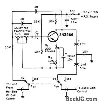
Can be added between product detector and volume control of SSB receiver or transceiver that does not have CW filter. Just before oscillation oceurs, gain becomes extremely high with very narrow bandpass. Regeneration and bandpass can be adjusted as required. Filter typically has 40-Hz bandwidth centered on 800 Hz.-R. A. Yoemans, Further Enhancing the Yaesu FTDX-560 Transceiver, CQ, July 1972, p 16-18 and 20-22. (View)
View full Circuit Diagram | Comments | Reading(1587)
THREE_PHASE_1O_MC_CLOCK
Published:2009/7/11 3:06:00 Author:May
Used in digital computer circuit testing when recirculcttion of pulses and pulse regeneration and shaping are required. Delay line provides required impedance match.-R. W. Buchanan and B.Kautz, Dynamic Testing of Computer Building Blocks, Electronics, 32:33, p66-68. (View)
View full Circuit Diagram | Comments | Reading(587)
CW_FILTER
Published:2009/7/11 3:05:00 Author:May

Simple single-section parallel-tuned active filter uses negative-impedance converter or gyrator to replace hard-to-get inductor of passive code filter. Capacitor CL is gyrated from 0.0332 ptF to effective inductance of 1.87 H. Filter has 6-dB gain at resonance and essentially zero output impedance. Bandpass is 85 Hz centered at about 865 Hz. Uses single -12 V supply. Resistors R are 7.5K, matched to about 2%.-N. Sipkes, Build This CW Filter, 73 Mag-azine, June 1977, p 55. (View)
View full Circuit Diagram | Comments | Reading(984)
BANDPASS_FILTER_TESTER
Published:2009/7/11 3:03:00 Author:May

Measures center frequency of active bandpass filter by measuring phase angle as function of frequency. 0utput of VCO excites bandpass filter under test.Output of filter serves as input for PLL comparator. When VCO and filter signals are in phase, PLL Iocks at center frequency of filter, corresponding to 0°phase shift. Accuracy is 1% for measurements in AF range.-M. P. Prongue, Phase-Lock Loops Test Bandpass Filters, EDN Magazine, June 20, 1974, p 76 and 78. (View)
View full Circuit Diagram | Comments | Reading(1282)
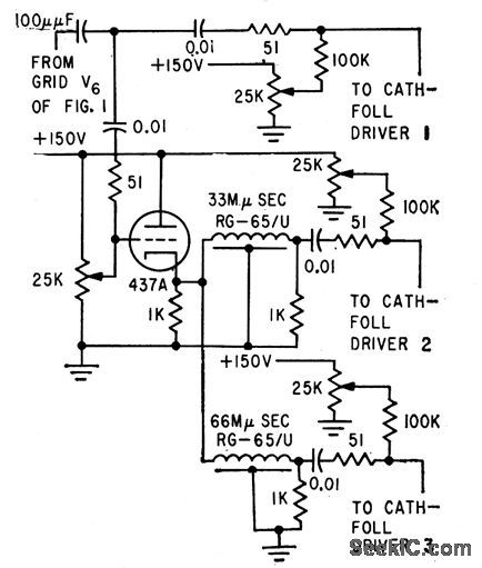
10_MC_CLOCK_OSCILLATOR
Published:2009/7/11 3:02:00 Author:May


Output through cathode follower is split into three channels(two are not shown) to get clock pulses at three phases.-G,O. Olson,Design of High-Frequency clock Pulse Generators Electronics,32:35,p56-57. (View)
View full Circuit Diagram | Comments | Reading(643)
VIDEO_LOOP_THRU_AMPLIFIER
Published:2009/7/11 3:02:00 Author:May
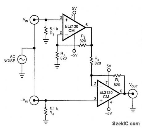
This video bandwidth amplifier rejects commonmode noise, such as 60- and 120-Hz hum. Bandwidth is typically 60 MHz for a differential gain of 2.The common-mode rejection is typically 45 dB.The design equations are:
ADIFF ≥ 1R2 = R4 (select both for optimum bandwidth)R1=R2 (ADlFF-1)R3=R4 (ADIEF-1) (View)
View full Circuit Diagram | Comments | Reading(658)
| Pages:779/2234 At 20761762763764765766767768769770771772773774775776777778779780Under 20 |
Circuit Categories
power supply circuit
Amplifier Circuit
Basic Circuit
LED and Light Circuit
Sensor Circuit
Signal Processing
Electrical Equipment Circuit
Control Circuit
Remote Control Circuit
A/D-D/A Converter Circuit
Audio Circuit
Measuring and Test Circuit
Communication Circuit
Computer-Related Circuit
555 Circuit
Automotive Circuit
Repairing Circuit