
Circuit Diagram
Index 778
ASCLL_TO_BAUDOT_CONVERTER
Published:2009/7/11 3:28:00 Author:May

Converts parallel ASCLL output of keyboard to serial Baudot format for driving Baudot teleprinters.conversion circuit can save several hundred bytes of computer or microprocessor storage,making this memeory space available for other purposes Article gives conversion table for for all capital and lowercase alphabetic characters,numeric,and punctuation.-J.ALehman and R.Graham,ASCLL to Baudot...er...Murray(the Hard Way ),Kilobaud,June 1978,p 80-83.
(View)
View full Circuit Diagram | Comments | Reading(918)
FAILURE_MONITOR
Published:2009/7/17 2:38:00 Author:Jessie

Some time ago, a situation arose in which a watchdog timer was needed to monitor an embedded computer. The computer in question required approximately 2 1/2 minutes to boot up and run the application software, so a monitor circuit was created that could wait 3 minutes before indicating failure. U1A, U2A, U2B, and U3 form a 3-minute timer. U1A operates as a free-running oscillator with a period of 1.41 s. The square-wave pulses are counted by U3, which generates an oscillator reset via U2A that effectively stops the clock. During the 3-minute interval, U2C and U2D send the oscillator signal to DS1, causing the indicator to flash. This flashing shows that the equipment is in its power-up cycle. When the reset occurs, the output of U1A is held low. U2B is a power-up reset for the counter. After 3 minutes, the indicator will come on continuously unless the watchdog input signal is present. U1B is configured as a 3.3-s-duration one-shot. When the watchdog input is pulsed low, the output switches high and keeps the LED from turning on. If the next pulse is not received in at least 3.3 s, the output will remain low. As a result, the LED will turn on, indicating failure. Should the watchdog input begin pulsing prior to the 3-minute timer, the watchdog will take precedence and turn off the flashing LED.What happens if the watchdog circuit fails? One of the characteristics of the NE556 timer is the inability to fully discharge the timing capacitor if the timer is retriggered prior to finishing a timing cycle. Applying a 10-Hz, 100-ms-wide pulsed input to the watchdog causes the capacitor charge to accumulate for approximately 8 s. This results in a 100-ms heartbeat flash of the LED every 8 s, which indicates that the circuit is still alive and that the LED hasn't burned out. The watchdog input is generated by an I/O line of the computer. Depending on the I/O board's design, the signal might need to be inverted to allow the watchdog input to remain normally high. (View)
View full Circuit Diagram | Comments | Reading(787)
KEYER_SPEED_CONTROL
Published:2009/7/11 3:27:00 Author:May

Electronic time base provides direct readout of keyer speed for 5 to 40 WPM in increments of 5 WPM by noting positions of three speed-control switches. Vemier adjustment pot R1 can be used for continuous speed adjustment if desired. Analog frequency meter provides alternate direct indication of keyer speed on milliammeter that can be call.brated in words per minute. Frequency of NE555 oscillator is 100 times keyer speed. Keyer clock is obtained by dividing oscillator speed by 120; thus, for 24 WPM oscillator runs at 2400 Hz which can be read easily on digital counter.Time-base divider would supply 20-Hz clock frequency for 24-WPM keying.-G. Jones, Calibrated Electronic Keyer Time Base, Ham Radio, Aug. 1975, p 39-41. (View)
View full Circuit Diagram | Comments | Reading(619)
Programmable_gain_bridge_transducer_amplifier_
Published:2009/7/17 2:37:00 Author:Jessie

Programmable gain bridge transducer amplifier (courtesy Analog Devices, Inc.). (View)
View full Circuit Diagram | Comments | Reading(624)
REMOTE-CONTROLLED_SWITCHER
Published:2009/7/11 3:27:00 Author:May


The interface end of Fig. 96-2(a)'s circuit deliver 10 V down the cable, pulses the supply voltage to transmit channel-change commands, and buffers the received video signal.The multiplexer circuit in Fig. 96-2(a) receives power and control signals over the coaxial cable, while driving the cable with the currently selected video signal.The interface circuit (Fig. 96-2(b)) delivers 10 V to the cable and pulses the supply voltage to select one of 8 channels. When the send button is depressed, a digital burst of 1.2 V amplitude (negative) is superimposed on the 12-V line (as a voltage drop). This does not affect the video signal. The multiplexer circuit (Fig. 96-2(c)) consists of a multiplexer and an amplifier. The multiplexer is a Maxim MAX455. The digital code on the supply line is picked off by A1, IC3A, and interfaced to counter IC2, which drives the multiplexer to select the desired video channel. (View)
View full Circuit Diagram | Comments | Reading(966)
ELECTRONIC_CHRONOMETER
Published:2009/7/11 3:24:00 Author:May

Trimmers permit adjusting timing by a few seconds per year.Major error is due to aging of quartz crystal,Tunnel diodes divide 100-kc crystal frequency by 2,000 to give 50-cps output for driving motor of clock.-R. L. Watters, Tunnel Diodes Control Quartz-Crystal Chronometer, Electronics, 34:39, p129-131. (View)
View full Circuit Diagram | Comments | Reading(589)
DENSIIOMETER
Published:2009/7/17 2:37:00 Author:Jessie

Used in scanning X-ray diffraction photograph and measuring densities of hundreds of spots. Circuit integrates point-by-point values of optical extinction over the required area of the negative.-E. M. Dooley, Flying-Spot Integrating Densitometer, Electronics, 34:3, p 64-66. (View)
View full Circuit Diagram | Comments | Reading(1971)
KEYER_OSCILLATOR
Published:2009/7/11 3:24:00 Author:May

Oscillator or clock starts when key is closed and can be held until dot, dash, or space is completed. U1 is SN7400, and U2 is SN74L04. Diodes at input of U2A form OR gate that controls oscillator. These inputs can be used to keep oscillator running for self-completing action. Time constant, set by C1 and R1, is 4 ms which is width of clock pulse. Values for C2, R2, and R3 give pulse repetition rate of 50 to 95 ms, comesponding to about 12 to 24 WPM.For higher speeds, reduce values of C2 and R2.CR1 and CR2 are signal diodes that prevent first pulse from being different; 250-pF capacitor on output prevents noise spikes from triggering keyer circuits falsely.-J. T. Miller, Integrated-Circuit Oscillator, Ham Radio, Feb. 1978, p 77. (View)
View full Circuit Diagram | Comments | Reading(1251)
0_15_V_BENCH_SUPPLY
Published:2009/7/17 2:36:00 Author:Jessie
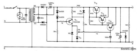
Provides up to 175 mA with ripple less than 1 mV. Choose Tr2 to handle load current. Current limiting is provided by 5.6-ohm (5R6) resistor and D1;when resistor drop exceeds about 1.2 V, current source Tr1 produces less current and output voltage is reduced.-J. A. Roberts, Bench Power Supply, Wireless World, May 1973, p 253. (View)
View full Circuit Diagram | Comments | Reading(884)
SHORT_PROTECTION_AND_SHUTDOWN_CIRCUIT
Published:2009/7/17 2:36:00 Author:Jessie
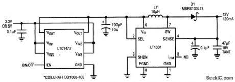
An LT1301 is used in the figure to boost a 3.3-V or 5-V input to 12 V, as for Vpp for flash memory. Although the LT1301 features a shutdown control, the input supply can still feed through to the output through L1 and D1. Similarly, a short circuit on the output could drag down the input supply. With the addition of the LTC1477, the circuit furnishes 100-percent load shutdown and output short-circuit protection. (View)
View full Circuit Diagram | Comments | Reading(597)
Bridge_amplifier
Published:2009/7/17 2:36:00 Author:Jessie

Bridge amplifier. Typical supply voltage is ±15 volts (courtesy Analog Devices, Inc.). (View)
View full Circuit Diagram | Comments | Reading(0)
Bridge_linearization_function_circuit_using_an_AD534_multiplier_divider_chip
Published:2009/7/17 2:35:00 Author:Jessie
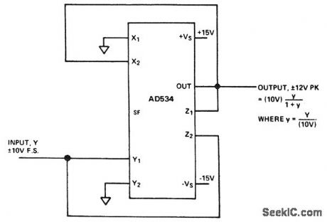
Bridge linearization function circuit using an AD534 multiplier/divider chip (courtesy Analog Devices, Inc.). (View)
View full Circuit Diagram | Comments | Reading(551)
80_METER_CW_DIRECT_CONVERSION
Published:2009/7/11 3:23:00 Author:May

Resonant-dipole antenna feeds directly into balanced product detector that cancels strong interfering local broadcast signals but adds products of mixing with local oscillator that covers 3490-3660 kHz for CW work. R3 is adjusted only once for best performance. Only half of GE GEL277 dual power amplifier is used, for gain of 40 dB. Circuit values make AF amplifier resonate at 1 kHz,with 12dB of attenuation per octave on either side of this center frequency.T1 should be shielded against vertical-sync magnetic fields of TV sets up to 60 feet away.T1 is transistor push-pull output transformer.Use twisted pair for connecting 1-1 and 2-2, to prevent imbalance effects. Article gives construction details for L1-L4.-B. Pasaric, A New Front End for Direct-Conversion Receivers,QST,Oct 1974,p 11-14. (View)
View full Circuit Diagram | Comments | Reading(1992)
AMPLIFIER_PROTECTOR
Published:2009/7/17 2:34:00 Author:Jessie
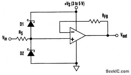
Unprotected amplifiers in noninverting, single-supply, voltage-follower stages might need external protection if input signals can exceed the rail voltages. Low-threshold Schottky diode clamps D1 and D2 provide safe clamping while RS limits the fault current. (View)
View full Circuit Diagram | Comments | Reading(870)
MULTIPLIER_SIMULATING_VOLTAGE_CONTROLLED_RESISTOR
Published:2009/7/17 2:33:00 Author:Jessie

A two- or four-quadrant multiplier can be configured to simulate a resistor with a value that is the ratio of a fixed resistor and a control voltage. If the voltage-controlled current source is made to depend on input voltage Vin (i.e.by driving Y2), as well as being allowed to float on top of Vin(i.e. by connecting Y2 to Z), then the input of Y2 will simulate a resistor with the transfer function Rin= R(U/Ec). One node of the simulated resistor will always be referred to ground. (View)
View full Circuit Diagram | Comments | Reading(857)
CMOS_KEYER_2
Published:2009/7/11 3:22:00 Author:May

Gives variable speed, automatic spacing, and self-completing dots and dashes.Gates C, B, and Aform gated MVBR Dot paddle initiates dot by making output of gate D go low, while gate E goes low for dash. Character-shaping section (gates G, H, and F with JK flip-flops FF1 and FF2 takes square pulses from pin 3 of MVBR gate B and gives perfectly spaced dots and dashes. FF1 divides clock pulses by 2, making dot equal to one complete period of MVBR. FF2 divides output of FF1 by 2, and outputs of both flip-flops are logically ORed to provide dashes. K1 is SPST reed relay. Supply can be 9-V battery.-T. R. Crawford, A Low-Power Cosmos Electronic Keyer in Two Versions, CQ, Nov. 1975, p 17-24. (View)
View full Circuit Diagram | Comments | Reading(930)
REMOTE_SELECTION_VIDEO_SWITCH
Published:2009/7/11 3:21:00 Author:May

The A/B Switch circuit consists of three ICs and a handful of resistors. Two gates from a 4011 quad 2-input NAND gate (U1A and U1B) are configured as a monostable multivibrator that, when switch S1 is pressed, triggers a 4017 decade counter/divider, which has been set to recycle after a count of two. The outputs of U2 at pins 2 and 3 are fed to the control inputs of U3 (a 4066 quad bilateral syritch) at pins 12 and 13. Depending on which control input is high, either the J1 or J2 output is selected.With a little modification, the switch could be set to trigger at a set rate (automatically). With the addition of another 4066, it could have as many as 8 channels. One possible application would be in a security surveillance system. (View)
View full Circuit Diagram | Comments | Reading(1913)
ELECTRONIC_CIRCUIT_BREAKER
Published:2009/7/17 2:33:00 Author:Jessie
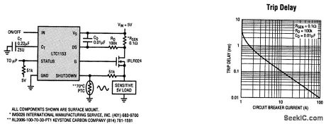
Fault conditions can quickly put stress on power sources and also on the loads themselves. Without a protective device to interrupt power during fault conditions, the supply can be overloaded or a load can overheat. The LTC1153 is a high-side MOSFET switch controller device with built-in circuit breaker, which turns off the MOSFET switch in the event of a fault. There is a built-in automatic reset, along with an input for thermal shutdown. The trip delay and reset times are fully adjustable. Because of its low (20 μA max) standby current, the LTC1153 can also be used in battery-powered equipment to protect the battery without reducing battery life. The switch can also be controlled with logic input. A status indicator reports fault conditions to a processor. (View)
View full Circuit Diagram | Comments | Reading(1156)
SIDEREAL_REGENERATIVE_OSClLLATOR
Published:2009/7/11 3:19:00 Author:May

Compares synchronous clock motor speed at 30-sec intervals with pendulum-driven master sidereal-time clock. Motor runs slightly faster than sidereal lime. If too fast at checking time, check capacitor at input of V1 is closed to reduce frequency of oscillation ond speed of motor to bring it back into coinddence with master.-C.N. Kingston, Radio Telescope Sees 2 Billion Light Years, Electronics, 31:23, p70-75. (View)
View full Circuit Diagram | Comments | Reading(684)
NANOAMPERE_SENSING_CIRCUIT
Published:2009/7/17 2:33:00 Author:Jessie

May be used as sensitive current detector or as voltage detector having high input impedance. Circuit input impedance is 100 meg. Input current of 40 nanoamperes charges C2 and raises emitter voltage of 2N494C to trig goring level. C1 and C2 then discharge, and resulting positive pulse triggers scr or other pulse-sensitive circuitry.-Transistor Manual, Seventh Edition, General Electric Co., 1964, p 326. (View)
View full Circuit Diagram | Comments | Reading(1154)
| Pages:778/2234 At 20761762763764765766767768769770771772773774775776777778779780Under 20 |
Circuit Categories
power supply circuit
Amplifier Circuit
Basic Circuit
LED and Light Circuit
Sensor Circuit
Signal Processing
Electrical Equipment Circuit
Control Circuit
Remote Control Circuit
A/D-D/A Converter Circuit
Audio Circuit
Measuring and Test Circuit
Communication Circuit
Computer-Related Circuit
555 Circuit
Automotive Circuit
Repairing Circuit