
Circuit Diagram
Index 765
MODEM_PROTECTION_CIRCUIT
Published:2009/7/17 2:32:00 Author:Jessie
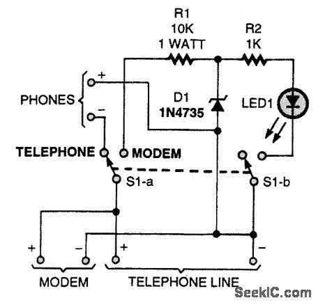
A common problem in modem communications is that family members often pick up extensions during a modem call. Forget about having your downloads messed up by someone lifting a phone.This circuit completely disconnects all phones on a line when you are using a modem. (View)
View full Circuit Diagram | Comments | Reading(572)
SOLID_STATE_TURNOFF_DELAY
Published:2009/7/12 20:45:00 Author:May
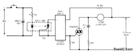
Designed for applications where machine must remain energized for certain period of time after some other operation has stopped, as when pump motor must run long enough to dear pipes in chemical plant. When switch is closed, LED of optoisolator is forward-biased and turned on, making photoGCR conduct and provide gate current via MDA920-4 diode bridge fortriac. Values shown keep solid-state relay circuit on for about 5 s after pushbutton is released. Resistor and capacitor values can be changed to obtain different delay.-T. Mazur, Solid-State Relays Offer New Solutions to Many Old Problems, EDN Magazine, Nov. 20, 1973, p 26-32. (View)
View full Circuit Diagram | Comments | Reading(620)
TOUCH_OPERATED_CODE_PRACTICE_OSCILLATOR
Published:2009/7/12 20:43:00 Author:May

A touch-operated CPO is shown in the figure. The gates of IC1-a are biased high through the two 22-MΩ resistors (R1 and R2), keeping its output low. Gates IC1-b and IC1-c are connected in an audio oscillator circuit that can operate only when pin 5 of IC1-b is high. The last gate of the 4093, IC1-d, adds isolation to the oscillator's circuit and drives the speaker (SPKR1). Touching the key paddle and ground plane lowers IC1-a's input gate voltage to near zero, allowing the output at pin 3 to go high. The tone generator then turns on and sends out an audio note. The touch key paddle and ground plane can be made from a circuit board or any other conductible material. Note that the ground plane should lie flat for a hand rest and the key paddle should be positioned for ease of touch. (View)
View full Circuit Diagram | Comments | Reading(855)
MEMORY_DRIVER_AND_READOUT_AMPLIFIER
Published:2009/7/12 20:41:00 Author:May

Used with tunnel-diode memory operating 5 Mc.-S. Takahashi and O. Ishii, High-Speed Memory Uses Tunnel Diode Circuit, Electronics,34:42, p66-68. (View)
View full Circuit Diagram | Comments | Reading(515)
PLL_CODE_PRACTICE_OSCILLATOR
Published:2009/7/12 20:41:00 Author:May

This CPO usesa 567 phase-locked loop, IC1, as the variable tone generator. The oscillator's frequency is set by R6, and the frequency range can be changed by selecting a different-value capacitor for C5. To lower the oscillator's frequency range, make the value of C5 larger, and to increase the frequency range, reduce C5. A general-purpose 2N3906 PNP transistor, Q1, supplies power to the 567 through pin 4 each time that the CW key is closed. Meanwhile, Q2, a general-purpose 2N3904 NPN transistor, buffers the oscillator's output and drives the speaker. Potentiometer R7 sets the output volume. (View)
View full Circuit Diagram | Comments | Reading(995)
ORYSTAL_CONTROLLED_CODE_PRACTICE_TRANSMITTER
Published:2009/7/12 20:39:00 Author:May
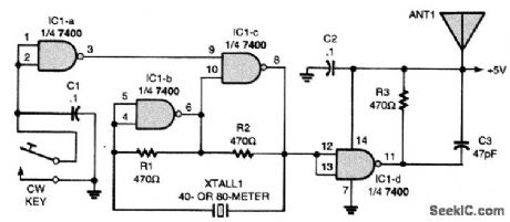
When the CW key is closed, IC1-a's output goes high, allowing IC1-b and IC1-c to oscillate. The crystal supplies the feedback path setting the oscillator's operating frequency. The circuit will operate on the 40- and 80-m bands. Section IC1-d isolates the oscillator from the short antenna, ANT1. A clip lead should do here to get the signal out and about for operation. Tune your ham-band receiver to the crystal's frequency and key down. If the receiver doesn't have a CW mode, turn on the BFO and tune for the desired CW tone. (View)
View full Circuit Diagram | Comments | Reading(723)
DRIVE_FOR_THIN_FILM_MEMORY
Published:2009/7/12 20:38:00 Author:May

Has single pulse output when input blocking oscillator is triggered by single positive-going pulse, for driving film alternately from one remanence to another in astatic loop.-S. Feinstein and H. J. Weber, Electrical Readout from Thin Ferromagnetic Films, Electronics, 33:31, p100-102. (View)
View full Circuit Diagram | Comments | Reading(612)
MORSE_CODE_OSCILLATOR
Published:2009/7/12 20:38:00 Author:May

The circuit is built around a 555 oscillator (IC1) and an LM386 audio amplifier (IC2). The 555 circuit is an astable oscillator, with the chip output retriggering the circuit. When the key (S1) is pressed, it activates the circuit. The 555 oscillates at a frequency determined by R1, R2, and C1. Potentiometer R2 is used to adjust the tone frequency of the oscillator. Some of the output current of IC1 is coupled to IC2 via a 10-°F capacitor, C2, so that it will be sufficient to drive a loudspeaker. Because the circuit has no gain control, the volume depends on the size and wattage of the speaker. (View)
View full Circuit Diagram | Comments | Reading(2285)
DIGITAL_VOLUME_CONTROL
Published:2009/7/12 20:37:00 Author:May

The heart of the digitally operated volume control is IC2, a 4067 16-channel analog multiplexer. Depending on the logic state on pins A, B, C, and D of the multiplexer, one of its 16 inputs or outputs is connected to pin 1, which is the wiper of the control. Because a 1-kΩ resistor has been connected between each input and output, the multiplexer can be considered a linear potentiometer with 16 fixed steps. Its overall resistance is 15 kΩ. It is, of course, possible to use a different value for each of the resistors to obtain a different characteristic. The setting of the potentiometer is controlled by counter IC1. Dependent on the position of switch S1, the counter moves one step up or down when switch S1 is changed over. Circuits IC3A and IC3B debounce S2.A jump from 0000 to 1111 or the other way around is not possible, because further count pulses are suppressed with the aid of the CO line. This line is logic low when both the counter state and signal U/D are 0.When U/D is high and the counter state is 15, COagain becomes logic low. It is then necessary to reverse the logic state at U/D, and thus the direction of counting. The volume control draws a current of around 1 mA. (View)
View full Circuit Diagram | Comments | Reading(5241)
HALF_ADDER
Published:2009/7/12 20:36:00 Author:May
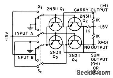
Uses four-point matrix of pnp junction switching transistors, whh bases and emitters cross-connected. Input A can be switched to base of Q1 or Q2. Input B can be switched between two alternate sets of emitters. For any input switch position, only one transistor is conducting.-F. B. Maynard, Half-Adders Drive Simultaneous Computer, Electtonics,31:29,p80-82. (View)
View full Circuit Diagram | Comments | Reading(1047)
SIMPLE_52_kHz_CLOCK
Published:2009/7/12 20:36:00 Author:May
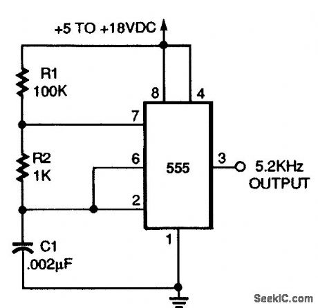
This circuit will produce a clock signal of 5.2 kHz using a NE555 timer. (View)
View full Circuit Diagram | Comments | Reading(583)
TIME_COMPARATOR
Published:2009/7/12 20:35:00 Author:May
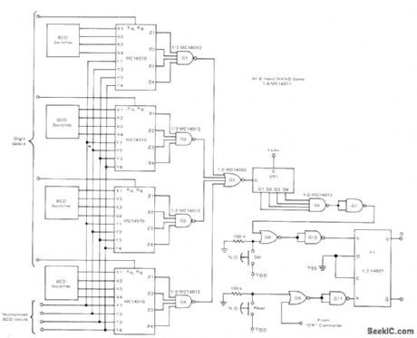
Digital circuit compares time that has been preset on one set of BCD input switches to multiplexed BCD output of basic 24-h industrial clock. When time of day corresponds to preset tifne, output circuit of comparator turns controlled device on for preset period of time. Second set of comparators can be used to tum device off when time of day equals preset time. Only hour and minute digits are compared, using Motorola MC145194-bit AND/OR select ICs, Q output of F1 can be used to control load power through output control circuit driving triac, with optoisolator providing required isolation from AC line. Supply is +5 V.-D. Aldridge and A. Mouton, Industrial Clock/Timer Featuring BackUp Power Supply Operation, Motorola, Phoenix, AZ, 1974, AN-718A,p6. (View)
View full Circuit Diagram | Comments | Reading(1062)
LOW_POWER_WIDE_SUPPLY_RANGE_CLOCK
Published:2009/7/12 20:34:00 Author:May
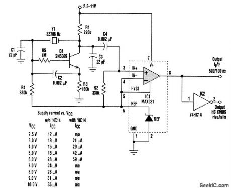
This 32-kHz, low-power clock oscillator offers numerous advantages over conventional oscillator circuits based on a CMOS inverter.Many times, 32-kHz oscillators are used to generate a system clock or an auxiliary sleep clock in low-power instruments and microcontrollers. The typical implementation uses a CMOS inverter (74HC04 or CD4049UB type). Inverter circuits present problems, though. Supply currents fluctuate widely over a 3- to 6-V supply range, and currents below 250 μA are difficult to attain. Operation can be unreliable for wide variations in supply voltage. A very low power crystal oscillator solves these problems. Drawing only 13μA from a 3-V supply, it consists of a single-transistor amplifier/oscillator (Q1) and a low-power comparator/reference device (IC1). Q1's base is biased at 1.25V via R5, R4, and the reference in IC1. VBE is about 0.7 V, placing the emitter at approximately 0.5 V. This constant voltage across R3 sets the transistor's quiescent current at 5μA, which fixes the collector voltage at about 1 V below VCC. The amplifier's nominal gain (R1/R2) is approximately 2 V/V The crystal and load capacitors (C1 attd C3) form a feedback path around Q1, whose 180°of phase shift causes the oscillation. C4 couple this singal to the comparator input;the input's quiescent voltage (1.25V) is set by the reference via R2.The comparator's input swing is thus centered around the reference voltage. Operating at 3V and 32 KHz,IC1 draws about 7μA. (View)
View full Circuit Diagram | Comments | Reading(1676)
SHORT_WAVE_RECEIVER
Published:2009/7/17 2:32:00 Author:Jessie

Using a Signetics NE602 in a varactor-tuned front end, the circuit of a shortwave receiver can be very simple and yet give high performance. This circuit also uses a ceramic filter as a sensitivity-determining device, two IF stages, AGO, and an audio amplifier. It has a sensitivity of under 1μV. The table shows coil data for the frequencies from 5 to 16 MHz. The values C18, C19, and C23 depend on the frequency range chosen. (View)
View full Circuit Diagram | Comments | Reading(3696)
CLOCK_GATE
Published:2009/7/12 20:32:00 Author:May


Provides effective gating with negligible insertion loss. Used as part of clock driver for developing and testing large digital computers.-S.Schoen,Transisitors Provide Computer Clock Signals.Electronics.32:9,p70-72 (View)
View full Circuit Diagram | Comments | Reading(639)
AMMETER_FOR_PRlNTEDCIRCUIT_WIRING
Published:2009/7/12 20:30:00 Author:May
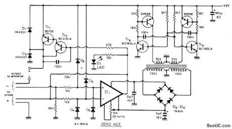
Permits measurement of current in single conductor on board without cutting it. Article gives design of probe having four projecting wires that are pressed on conductor being measured, and describes operation of circuit in detail. Opamp can be 741, but higher-cost 725C will improve performance, When all four wires of probe make contact, voltage drop appears at input of differential amplifier. Outer wires of probe carry current of opposite polarity passing through ammeter; because there is negative feedback loop in conductor, opamp input voltage will return to zero when outgoing current is equal to that of unknown current passing through printed-circuit conductor.-F. An-drews, P.C.B. Ammeter, Wireless World, July 1976, p 34. (View)
View full Circuit Diagram | Comments | Reading(834)
LIQUID_LEVEL
Published:2009/7/17 2:31:00 Author:Jessie
Nonconducting liquids change electrostatic capacitance of ring electrodes in tank. Amplified error signal from electrode bridge operates recording galvanometer or indicator lamps to provide measurements of level accurate to 0.01 inch.-T. L. Greenwood, Capacitance Change Indicates liquid Levels, Electronics, 33;34, p 66-67..
(View)
View full Circuit Diagram | Comments | Reading(740)
ARITHMETIC_CELL
Published:2009/7/12 20:28:00 Author:May

Uses 27 resistively-coupled tunnel diodes, powered from three-phase pulse supply. Repetition rate is 1 Mc.-T, Maguire, Computers Head for 1,000-Mc Opercttion, Electronics, 33:5, p55-59. (View)
View full Circuit Diagram | Comments | Reading(765)
POWER_SUPPLY_PASS_TRANSISTOR_PROTECTION_CIRCUIT
Published:2009/7/17 2:31:00 Author:Jessie
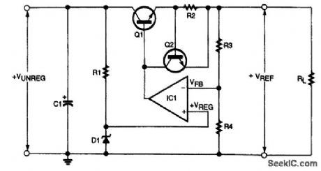
A current-limiting transistor and resistor protect the pass transistor and rectifier bridge in this linear supply. (View)
View full Circuit Diagram | Comments | Reading(847)
TRANSISTOR_TESTER_2
Published:2009/7/12 20:28:00 Author:May
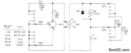
Useful for troub:eshooting and forchecking small-slgnal transistors having no markings Set four-pole five-position rotary switch S2 to SHORT(lowestpostion) before inserting transistor,then flip S1 back and forth,If meter shows any reading at all,reject transistor without further tests,rmeter stays at zero,set S2 to ICBO(conector-base current, emitter open). Discard transistor if reading is high foreither position of S1; modern transistors pass only nanoamperes, but older types may give noticeable reading, particularly if germanium. Repeat test for ICEO (collector-emitter current, base qpen), which should be greater than ICBO by factor approximating curtent gain (beta) of device, Modern silicon transistors may give no reading here. For final beta test, older types show 100 or less and modern transistors like 2N3391 have beta readings between 300 and 400. CR1 is 1N4603.-D. Cheney, Shirt Pocket Transistor Tester, Ham Radio, July 1976, p 40-42. (View)
View full Circuit Diagram | Comments | Reading(1134)
| Pages:765/2234 At 20761762763764765766767768769770771772773774775776777778779780Under 20 |
Circuit Categories
power supply circuit
Amplifier Circuit
Basic Circuit
LED and Light Circuit
Sensor Circuit
Signal Processing
Electrical Equipment Circuit
Control Circuit
Remote Control Circuit
A/D-D/A Converter Circuit
Audio Circuit
Measuring and Test Circuit
Communication Circuit
Computer-Related Circuit
555 Circuit
Automotive Circuit
Repairing Circuit