
Circuit Diagram
Index 766
PULSE_FREQUENCY_MODULATED_RECEIVER
Published:2009/7/17 2:31:00 Author:Jessie
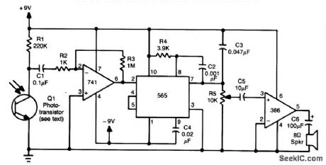
This receiver uses an IR-sensitive phototransistor (Clairex, HP, etc.) mounted in a light-tight enclosure with an aperture for the incoming IR beam. An optical system can be used with this receiver for increased range. A 741 amplifies the pulsed IR signal and a 565 PLL FM demodulator recovers the audio, which drives an LM386 audio amplifier and speaker. (View)
View full Circuit Diagram | Comments | Reading(1642)
RECIPROCAL_CIRCUIT
Published:2009/7/12 20:18:00 Author:May
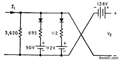
Output is inversely proportional to input. Article gives design procedure based on use of diodes, resistors, and d-c voltage supplies.-A. Gill, Procedure for Designing Reciprocal Computer Circuits, Electronics, 33:21, p92-93. (View)
View full Circuit Diagram | Comments | Reading(919)
SIMPLE_CIRCUIT_TO_DISCONNECT_LOAD_FROM_BATTERY
Published:2009/7/17 2:31:00 Author:Jessie

To prevent battery damage, the circuit disconnects the load at a predetermined level of load voltage. This level (Vtrip, closely proportional to the battery voltage) is determined by R1 and R2 so that the voltage at pin 3 of IC1 equals 1.15 V: Vtrip = 1.15 V(R1 + R2) /R1 The allowed range for Vtrip is 2 V to 16.5 V. The load-battery connection remains open until the system receives a manual reset command. Pressing Reset (or pulling pin 3 above 1.15 V with a transistor) reconnects the load after the battery is recharged or replaced. Battery drain with the load disconnected is only 5 μA, so the circuit can remain in that state for an extended period without causing a deep discharge of the battery. Choose Q1 for a minimal voltage drop (source to drain) at the required load current. (View)
View full Circuit Diagram | Comments | Reading(1705)
THIN_FILM_MEMORY_READOUT
Published:2009/7/12 20:14:00 Author:May


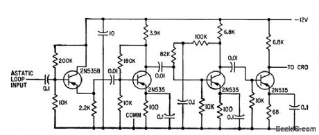
High-gain am plifier has gain of 65 db and produces saturated output for cro.-S. Feinstein and H. J.Weber,Electrical Readout from Thin Ferromagnetic Films,Electronics,33:31,p100-102. (View)
View full Circuit Diagram | Comments | Reading(616)
TRANSIENT_SWITCH_SIGNAL_SUPPRESSOR
Published:2009/7/17 2:30:00 Author:Jessie

The figure shows a circuit that delays the transmission of a switch-opening or switch-closing signal until after a preset suppression time. The circuit is used to prevent the transmission of an undesired momentary switch signal. For example, a pressure switch that is meant to be held steadily on or off by a given static pressure in a piping system can also be actuated momentarily by a transient overpressure (sometimes called water hammef') or underpressure caused by the sudden closure or opening of a valve. The basic mode of operation is simple. The beginning of the switch signal initiates a timing sequence. If the switch signal persists after the preset suppression time, then this circuit transmits the switch signal to the external circuitry. If the switch signal is no longer present after the suppression time, then the switch signal is deemed to be transient, and this circuit does not pass the signal on to the external circuitry. From the perspective of the external circuitry, it is as though there were no transient switch signal. The suppression time is preset at a value large enough to allow for the damping of the underlying pressure wave or other mechanical transient. (View)
View full Circuit Diagram | Comments | Reading(715)
VOLTAGE_TO-FREQUENCY_CONVERTER_WITH_OPTOCOUPLER
Published:2009/7/11 5:31:00 Author:May

In this circuit, a Raytheon RC4151 or National LM131 is used in conjunction with an optocoupler for applications where input-to-output isolation is desirable. Circuit values are shown in the figure for various applications. (View)
View full Circuit Diagram | Comments | Reading(2097)
OLD_TIME_RADIO
Published:2009/7/17 2:30:00 Author:Jessie

This circuit was used in the early days of radio to receive signals. Almost any battery-operated triode, such as a type 30, can be used. A battery is 3 V, R2 is a 100-Ω rheostat. Coils are typically 2 to 3 diameter honeycomb wound. (View)
View full Circuit Diagram | Comments | Reading(709)
SIMPLE_LOW_FREQUENCY_V_F_CONVERTER
Published:2009/7/11 5:28:00 Author:May

In this circuit, C1 is charged to a fixed reference level, then discharged. Integrator IC1 circuit charges C1 until IC1 has -6.2-V output, when comparator IC2 outputs a low. FET Q1, triggers one-section monostable multivibrator IC3, pulls pin 3 1ow for 470 μs, ensuring that Q1 completely discharges C1. The other section of IC3 produces a longer pulse of about 47 ms.Full scale of this circuit is 10 Hz. For lower output pulse rates, a counter circuit can be inserted between the sections of IC3. Notice that because C1 does not integrate while Q1 is biased on, this circuit has an error in the output period, which must be as short as possible. Therefore, the circuit's use is limited to low frequencies. (View)
View full Circuit Diagram | Comments | Reading(1534)
REVERSED_POWER_SUPPLY_PROTECTOR_CIRCUIT
Published:2009/7/17 2:29:00 Author:Jessie

This circuit is designed to sense a power-supply output (to other circuitry) and detect a reversed-polarity condition. The circuit consists of a complementary metal-oxide semiconductor (CMOS) decoder (CD4555B), which monitors the output of an external power supply for proper polarity. If the power-supply polarity is incorrect, the CD4555B detects that condition and triggers a 2N5060 SCR (Q1). After triggering, the SCR supplies current to a relay (K1), which, upon activation, changes the external power-supply connections (to the external circuitry) to the correct polarity and illuminates a light-emitting diode (LED) to provide a visual warning of the polarity-reversal condition. After the reversed-polarity condition is remedied, pressing the contact switch (S1) momentarily will reset the circuit to its original state. In its present configuration, the circuit can accommodate standard positive power supplies with dc voltages of +5, +10, + 12, and + 15 V. The decoder was designed to operate at these different voltages. With some modifications, the circuit can monitor and correct anomalous power-supply outputs from +3 V, +28 V, or negative-polarity power supplies, or voltages that are either too high or too low. (View)
View full Circuit Diagram | Comments | Reading(702)
WIRE_THICKNESS_GAGE
Published:2009/7/17 2:29:00 Author:Jessie
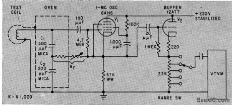
Uses principle of proximity detectors for nondestructive measurement of moving copper wire thickness during drawing operation or on coil-winding machine. Wire passing through test coilacts like shorted turn of transformer, lowering Q of coil. Stable 1-Mc oscillator and buffer drive vtvm that indicates variations in wire diameter for sizes down to AWG 46. -K. H. Jaensch, Wire Gage Provides Continuous Measurement, Electronics, 33;7, p 109-111. (View)
View full Circuit Diagram | Comments | Reading(1197)
POPCORN_NOlSE_TESTER
Published:2009/7/11 5:27:00 Author:May
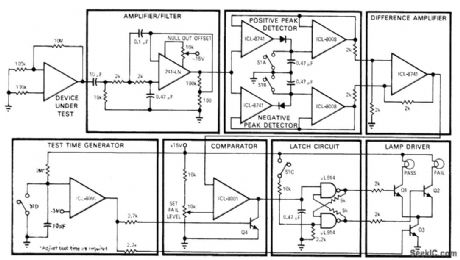
Developed at Intersil to test opamps for erratic low-frequency jumps between two or more stable states. After start-up switch S is closed, pass/fail lamps are inhibited by Q3. At end of preselected test time (typically 5 s), one of lamps will come on. If output from difference amplifier exceeds preset fail level at inverting input of comparator during test period, fail lamp is turned on by Q2. Q4 prevents triggering of latch by spurious signals after end of test time.-T. P. Rigoli, IC Op Amps, EDNMagazine, May 1, 1971, p 23-33. (View)
View full Circuit Diagram | Comments | Reading(785)
VOLTAGE_LEVEL_MONITOR
Published:2009/7/11 5:26:00 Author:May

Over-or-under circuit provides output signal when d-c input voltage is over 12V or under 6v, for monitoring or alarm purposes, with no output during desired on condilion.-M. Merlen and D.Grossman, Interrogator Circuit Can Tell Good Data from Bad, Electronics, 37:20, p58-59. (View)
View full Circuit Diagram | Comments | Reading(871)
TRF_RADIO
Published:2009/7/17 2:29:00 Author:Jessie
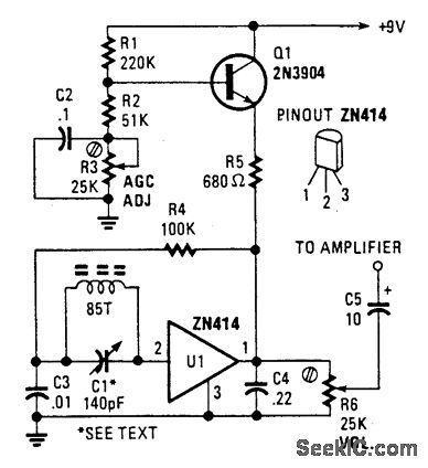
This simple AM radio uses a Ferranti ZN414 IC and runs from a 9-V supply. A 5/16 -diameter ferrite rod serves as an antenna, and uses about 85 turns of #28 enatnelled wire. (View)
View full Circuit Diagram | Comments | Reading(2251)
LONGWAVE_TRF_TUNER
Published:2009/7/17 2:29:00 Author:Jessie

This TRF tuner was intended for reception of Radio 4 AM broadcast signals in the United Kingdom on 198 kHz, with the best possible audio fidelity. It can be used as an IF amplifier or for reception of LW or MW AM broadcasts in other areas. The aerial wire is directly connected, via SK1, to the input tuned circuit (coil L1 and capacitors VC1 and C3) via a small-value capacitor C1. The second tuned circuit (L2, VC2, and C8) is similarly connected to the output from transistor TR2. The output from transistor TR3 is taken to the op-amp demodulator (IC1a) and also, via capacitor C9, to the diode-pump circuit D1/D2. The pump is used to generate a small negative AGC. For AM detection, if a diode is used as the rectifier, the tuner will not work very well on input volt-ages less than 0.5V peak. However, if a pair of diodes are hooked around an op amp, IC1a, as shown in the figure, the rectification threshold is reduced to a few millivolts, which increases the demodulator sensitivity by a few hundred times. The other half of the dual op amp, IC1b, is a straight AP amplifying stage, whose gain is adjustable by potentiometer VR1. Resistor R13 and capacitor C10, on its noninverting input (pin 5), act as a simple RE filter to remove any residual 198-kHz signal voltage from the audio output.
(View)
View full Circuit Diagram | Comments | Reading(1406)
AF_SIGNAL_TRACER
Published:2009/7/11 5:26:00 Author:May

Motorola MC1306P complementary power amplifier delivers 1/2 W into loudspeaker for 3-mVRMS input to preamp, for troubleshooting all types of audio equipment. Zero-signal current drain is only 4 mA with 9-V supply. For RF tracing of modulated AM or SSB signal, use demodulator probe at input.-W. M, Scherer, High-Gain Signal Tracer, CQ, July 1972, p 12 and 14. (View)
View full Circuit Diagram | Comments | Reading(1251)
SIMPLE_REVERSE_POLARITY_PROTECTION_CIRCUITS
Published:2009/7/17 2:29:00 Author:Jessie

Two methods to avoid damage to circuitry from reverse voltages using diodes are shown. (View)
View full Circuit Diagram | Comments | Reading(825)
REFLEX_RADIO_RECEIVER
Published:2009/7/17 2:28:00 Author:Jessie

The RF signal is passed from the antenna through C1 to the tuned circuit made up of L1 and C2.Oneend of L2 feeds the RF signal to the base of Q1 for amplification and the other end ties to the junction ofR1and R2 to supply bias to the transistor.A 0.02-μF capaotor,C3,places the“D”end of L1 at RE ground.
The amplified RF signal is fed through C6 to a two-diode doubler/rectifier circuit and then on to thevolume control,R6.The wtper of R6 feeds the detected audio signal through C9 to the junction of R1,R2,and the“D”end of u.The“D”end of L2 is at RF ground,but not AF ground,allowing the AF signal tobe passed through L2 to the base of Q1 for amplification. The junction of the 2.5-mH choke and T1 is placed at RF ground through C5. The amplified audio is fed from this junction to the mput ofthe 386 audioamplifier,U1,to drive the 4 8-Ω speaker.The single transistor has performed a dual duty by amplifying the RF and AM signals at the same time. (View)
View full Circuit Diagram | Comments | Reading(3103)
MOV_SURGE_PROTECTION_CIRCUIT
Published:2009/7/17 2:28:00 Author:Jessie

Three MOV devices (connected as shown) provide superior protection against line surges because all three legs are protected against excessive potential differences. (View)
View full Circuit Diagram | Comments | Reading(3029)
SHORT_CIRCUIT_SHUTDOWN_CIRCUIT
Published:2009/7/17 2:27:00 Author:Jessie

When a short or severe undervoltage develops, Q1 is cut off, deenergizing Q1, and disconnecting the load from the power supply. (View)
View full Circuit Diagram | Comments | Reading(717)
SIMPLE_CROWBAR_CIRCUIT
Published:2009/7/17 2:27:00 Author:Jessie

This circuit uses a zener diode and an SCR. When the supply voltage exceeds the zener break-down voltage plus the gate turn-on voltage of the SCR, current flows in the gate circuit, turning on the SCR and effectively shorting the supply. A fuse is generally placed in the supply line; it is designed to blow when the SCR fires, protecting and shutting down the supply. (View)
View full Circuit Diagram | Comments | Reading(1141)
| Pages:766/2234 At 20761762763764765766767768769770771772773774775776777778779780Under 20 |
Circuit Categories
power supply circuit
Amplifier Circuit
Basic Circuit
LED and Light Circuit
Sensor Circuit
Signal Processing
Electrical Equipment Circuit
Control Circuit
Remote Control Circuit
A/D-D/A Converter Circuit
Audio Circuit
Measuring and Test Circuit
Communication Circuit
Computer-Related Circuit
555 Circuit
Automotive Circuit
Repairing Circuit