
Circuit Diagram
Index 773
BIPHASE_WIDE-RANGE_VCO
Published:2009/7/11 4:21:00 Author:May

Using a CD4046B, this circuit generates abiphase signal.The frequency range is below 100Hz to about 1.5 kHz. (View)
View full Circuit Diagram | Comments | Reading(1863)
COHO_JITTER_MONITOR
Published:2009/7/17 3:01:00 Author:Jessie

Automatically monitors coherent oscillator frequency and provides visible indication of amount of jitter, as measure of mti system capability.-C. Clark, Checking Jitter in Moving Target Radar, Electronics, 32:29, p 56-58. (View)
View full Circuit Diagram | Comments | Reading(656)
DIODE_TESTER
Published:2009/7/11 4:20:00 Author:May

Developed to demonstrate how 0.002-μF shunt capacitor increases efficiency of diode detector. Can also be used to compare performance of different diodes, Input terminates AM signal generator. IC with associated capacitors and resistors forms low-pass filter having cutoff at 2 kHz. R1 is detector load. Resistor at output of U1 prevents oscillation of opamp when using coax feed to VTVM. For higher input signal levels, shunt capacitor in-creases AF output up to l0dB.-H. Olson, Diode Detectors, Ham Radio, Jan. 1976, p 28-34. (View)
View full Circuit Diagram | Comments | Reading(0)
ONE_CHIP_AM_RADIO
Published:2009/7/17 3:01:00 Author:Jessie

The ZN414 IC contains a complete AM radio, with AGC, except for an audio section. Like an MMIC, it is powered through its output terminal. (View)
View full Circuit Diagram | Comments | Reading(651)
IMPEDANCE_METER
Published:2009/7/11 4:19:00 Author:May

External AF voltage is applied to unknown impedance through input transformer T1 and calibrated variable resistor R1. Voltage drops across impedance and R1 are checked separately with electronic voltmeter while R1 is varied. When drops are equal, unknown impedance is equal to setting of R1, read directly from its calibrated dial. Voltmeter uses FET followed by two-diode rectifier X1-X2 and microammeter M1. With S2 in position A, volt-meter reads drop across R1 ; in position B, volt-meter reads drop across unknown impedance.Adjust R5 so meter deflection is near full scale to increase comparison accuracy. Common test frequencies used are 400, 500, and 1000 Hz.-R. P. Turner, FET Circuits, Howard W. Sams, Indianapolis, IN, 1977, 2nd Ed., p 143-144. (View)
View full Circuit Diagram | Comments | Reading(1946)
CAPACITOR_STORAGE_FEEDBACK_BOXCAR
Published:2009/7/11 4:17:00 Author:May

Improves accuracy of radar boxcar without sacrifice in speed, by using feedback principles to overcome instabilities in d-c offset voltages. Feedback forces boxcar output to equal input voltage during sampling, so intemal d-c offsets and instabilities Ionger than one storage interval are inconsequential. Box-car input goes to one terminal of difference amplifier, and boxcar output goes to other terminctl. Difference amplifer output is then used to control capacitor charge. By gating on difference ampliler during sampling interval, boxcctr output is made equcd to value of waveform at that time.-P. E. Harris and B. E. Simmons, DC Accuracy in a Fast Boxcar Circuit Via a Comparator, IEEE Transactions on Electronic Computers, June 1964, p 285-288. (View)
View full Circuit Diagram | Comments | Reading(754)
IMPROVED_REGENERATIVE_SW_RECEIVER
Published:2009/7/17 3:00:00 Author:Jessie

The figure shows the schematic of the circuit. A number of unique features give this design its trouble-free performance. The tendency for regenerative receivers to radiate oscillator-frequency signals is eliminated here by placing a transistor buffer Q1 between the antenna preselector circuit L1-C1a and the regenerative oscillator-tuned circuit L2-C1b. This buffer also nearly eliminates hand-capacitance effects. This design is also unique in that it uses an IC for the regenerative detector. U1, an LM1496 double-balanced mixer, is used here in a somewhat unorthodox manner. The differential SIGNAL INPUT amplifier transistors internal to the IC are used as a Hartley oscillator in conjunction with L2 and C1b. The regenerative feedback for this oscillator is supplied by the output of the GAIN and ADJUST pins of the LM1496. Some of the oscillator output is coupled to one of the CARRIER IN-PUT pins via C9, which allows the mixer section of U1 to act as an asynchronous detector, greatly improving the RE detection sensitivity over that of other regenerative circuits. The regeneration level is controlled by the voltage level applied to the BIAS pin of U1. The circuit containing R12 and transistor Q2 is used as a variable-voltage source, providing the regeneration level immunity from supply-voltage ripple. This bias level controls the quiescent current level through the SIGNAL IN-PUT amplifier transistors, which, in turn, determines the emitter output impedance of these transistors, controlling the amount of power delivered to the feedback winding of L2. This results in very smooth and predictable regeneration control. The outputs of U1 are coupled through audio trans-former T1 into the first section of U2, an LM324 op amp. Volume control is achieved though U2d and variable resistor R18. Using a push-pull audio output stage, as is done here, also reduces susceptibility to audio oscillation. Although the use of switched or plug-in coils could have allowed multiband reception, in the interest of simplicity, this was not done. However, the values of L1 and L2 allow coverage of 5 to 15 MHz, where much of the shortwave action occurs. (View)
View full Circuit Diagram | Comments | Reading(5077)
VOLTAGE_CONTROLLED_CURRENT_SINK
Published:2009/7/11 4:17:00 Author:May
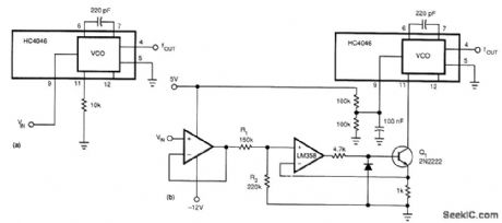
This circuit widens the linear frequency span of an HC4046 from one decade to nearly three decades. An LM358 is used as a constant-current sink to replace the frequency-determining resistor (10 kΩ) from pin 9 to ground. Pin 9 is held at a fixed 2.5 V for this application. (View)
View full Circuit Diagram | Comments | Reading(3065)
30_MHz_IF_AND_POWER_SUPPLY_FOR_10_GHz_GUNN_DIODE_COMMUNICATIONS_SYSTEMS
Published:2009/7/17 3:00:00 Author:Jessie

This unit consists of a TDA7000 IF amplifier and detector system,an LM386 audio amplifier,aCA3130 modulator circuit,a Gunn-diode supply( U7)that can be modulated with audio for production of wideband FM,and a 10-V regulator. (View)
View full Circuit Diagram | Comments | Reading(2103)
_VOLTAGE_TUNED_VHF_OSCILLATOR
Published:2009/7/11 4:08:00 Author:May

This VHF VCO circuit is suitable for 30 to 200 MHz. Q1 can be replaced by a 2N3563 for operation above 100 MHz. L1 is chosen to resonate to the desired frequency with the varactor capacitance of 40 pF. Other vatactors can be substituted or two back-to-back vat-actors can be used for better linearity, depending on the application. (View)
View full Circuit Diagram | Comments | Reading(2379)
AGC_amplifier
Published:2009/7/17 3:00:00 Author:Jessie
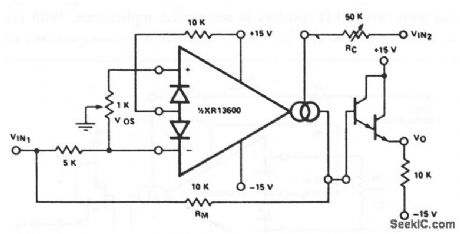
This circuit uses one section of an XR-13600 (Fig. 11-1B) as an AGC amplifier. When VO reaches a high enough amplitude to turn the Darlington transistors and linearizing diodes, the increase in ID reduces amplifier gain so as to hold VO at that level. The control point is set by RC and the output offset is adjusted by the 1 -kΩ potentiometer. (View)
View full Circuit Diagram | Comments | Reading(0)
Low_drift_integrator_with_low_leakage_guarded_reset
Published:2009/7/17 3:00:00 Author:Jessie

Low-drift integrator with low-leakage-guarded reset (courtesy Analog Devices, Inc.). (View)
View full Circuit Diagram | Comments | Reading(741)
KEYER_WITH_MEMORY_1
Published:2009/7/11 4:04:00 Author:May
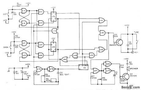
Features include dot and dash memory, gated clock, low standby and keydown currents, built-in sidetone oscillator with loudspeaker, and keying circuit for grid-block keyed transmitter. Will operate at least one year on 9-V transistor battery. Article describes circuit operation in detail. U1 is 4011 quad two-input NAND gate. U2 and U4 are 4081 quad two-input AND gates. U3 is 4013 dual D flip-flop. U5 is 4024 seven-stage binarv counter.U6 is 4071 quad two-input OR gate,U7 is 4001 quad two-input NOR gate,-E,A,Pfeiffer,MINIMOS-the Best Keyer Yet?,73 Magazine, Aug.1976,p 38-40 and 42-43. (View)
View full Circuit Diagram | Comments | Reading(725)
SWITCH_MODE_VOLTAGE_REGULATOR
Published:2009/7/17 2:59:00 Author:Jessie

Switch-mode power supplies offer the benefit of a much greater efficiency than obtainable with a tradi-tional power supply. The switch-mode regulator presented here has an efficiency of around 85%.
An input voltage of 12 to 16 Vdc is convened into a direct voltage of exactly 5 V. The use of a MAX638CPA enables the design and construction of the regulator to be kept fairly simple: only nine additional components are needed to complete the circuit.
Resistors R1 and R2 are used to indicate when the battery voltage becomes low: as soon as the voltage on pin 3 becomes lower than 1.3 V, D1 lights. With values as shown for the potential divider, this corresponds to the supply voltage getting lower than about 6.5 V. The output of the IC is shunted by a simple LC filter formed by L1, C3 and D2.
The oscillator on board the IC generates a clock frequency of around 65 kHz and drives the output transistor via two NOR gates. The built-in error detector, the battery low indicator or the voltage comparator can block the clock frequency, which causes the transistor to switch off.
The IC compares the output voltage of 5 V with a built-in reference (FET). Depending on the load, the FET will be switched on for longer or shorter periods. The maximum current through the FET is 375 mA, which corresponds with a maximum output current of 80 mA. (View)
View full Circuit Diagram | Comments | Reading(946)
RECEIVING_DISTRIBUTOR
Published:2009/7/11 4:03:00 Author:May
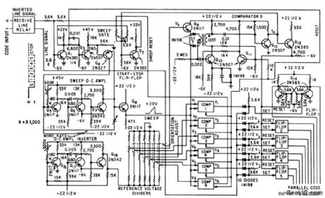
Converts tape-code input to 5-bit parallel code at five conventional flip-flops. Rising sweep voltage succes-sively triggers six comparator stages. If line signctl is positive at triggering time, flip-flop corresponding to triggered comparator is set to its one state. Used in high-speed electro-static printer in which each of 72 print heads has 35 print pins.-R,E,West,High-Speed Readout for Data Processing,Electronics,32:22,p83-85 (View)
View full Circuit Diagram | Comments | Reading(494)
RADAR_SPEED_METER
Published:2009/7/17 2:59:00 Author:Jessie

Translates doppler or difference frequency between transmitted and received frequencies into mph and displays on meter or records on strip chart. Operates at 2,455 Mc and is accurate within 2 mph up to 100 mph.-J. Barker, Radar Metet Helps Enforce Traffic Laws, Electronics, 32:10, p 48-49. (View)
View full Circuit Diagram | Comments | Reading(750)
CURVE_TRACER
Published:2009/7/11 4:02:00 Author:May

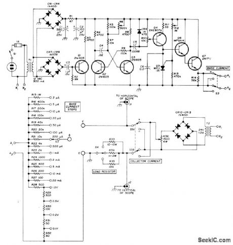
Displays on CRO a family of six collector characteristics for transistors and voltage/current characteristics of diodes, Circuit varies base voltage in discrete steps while sweeping collector voltage from zero to maximum at each step. Collector voltage is 120-Hz rectified sine wave from bridge rectifier CR10 CR13, varied by R36. S5 selects proper polarity. Base voltage steps are synchronized to 120-Hz colleetor voltage by adjusting R6 in mono MVBR Q2-Q3 driven by Q1. R10 adjusts voltage between steps. Programmable UJT Q5 resets staircase generator to zero. R12 adjusts gate voltage. Staircase voltage is coupled to bias resistors R15-R32 fortest transistor by Q6 and Q7, with bias polarity and value selected by S2 and S3. Connect device undertest to points B, C, and E. Connect points A1 and A2 together. R15-R35 should have 5% accuracy.-D. Wright, Transistor Curve Tracer, Ham Radio, July 1973, p 52-55. (View)
View full Circuit Diagram | Comments | Reading(3036)
LOW_LEVEL_CURRENT_DETECTOR_AND_MEMORY
Published:2009/7/17 2:59:00 Author:Jessie

Unknown current Ix charges C1, 0percttion of relay K1 by interrogate pulse discharges C1 through tunnel diode, initiating switching of diode if in low-voltage state and unknown current is correct polarity. Lamp in transistor amplifier glows when tunnel diode is in high-voltage state. Currents of one picoampere can be measured.-C. D. Todd, Tunnel Diode Detects Currents Down to 100 Femtoamperes, Electronics, 36:14, p 33-37. (View)
View full Circuit Diagram | Comments | Reading(727)
Four_quadrant_multiplier
Published:2009/7/17 2:58:00 Author:Jessie
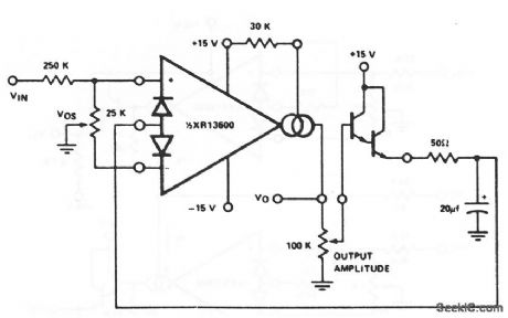
This circuit uses one section of an XR-13600 (Fig. 11-1B) as a four-quadrant multiplier. Notice that the output is taken from the amplifier, and that the buffer output is returned to the amplifier input. The 100-kΩ potentiometer sets the output amplitude and the 25-kΩ potentiometer is used to adjust offset. (View)
View full Circuit Diagram | Comments | Reading(0)
LINEAR_VCO
Published:2009/7/11 4:02:00 Author:May

This VCO uses an LF356 op amp to produce a linear frequency vs. voltage characteristic using the CMOS HC4046. The frequency range can be changed by changing the capacitor connected between pins 6 and 7 of the HC4046. Using the HC4046's internal transistor instead of an external component achieves the linearization in Fig. 98-5(b). (View)
View full Circuit Diagram | Comments | Reading(3049)
| Pages:773/2234 At 20761762763764765766767768769770771772773774775776777778779780Under 20 |
Circuit Categories
power supply circuit
Amplifier Circuit
Basic Circuit
LED and Light Circuit
Sensor Circuit
Signal Processing
Electrical Equipment Circuit
Control Circuit
Remote Control Circuit
A/D-D/A Converter Circuit
Audio Circuit
Measuring and Test Circuit
Communication Circuit
Computer-Related Circuit
555 Circuit
Automotive Circuit
Repairing Circuit