
Circuit Diagram
Index 760
PULSE_FORMER_AND_SHAPER
Published:2009/7/17 1:44:00 Author:Jessie

Converts sine-wave input to 40 millimicrosec output. Used in versatile pulse generator for testing high-speed computer circuits. Input frequency range is 3 to 20 Mg.-L. Numann Transistorized Generator for Pulse Circuit Design, Electronics, 32:14, p 47-49. (View)
View full Circuit Diagram | Comments | Reading(528)
PC_WATCHDOG
Published:2009/7/12 21:51:00 Author:May

The watchdog is intended to monitor a microprocessor and determine whether it functions correctly or not. It and its software are suitable for use in the background with any PC that runs under DOS or Windows. The hardware is linked to the serial interface, which is then controlled by the software. After the computer has been switched on, the data connections at the serial interface are low.The watchdog software is started at the same time as the selected application program. It provides a permanent rectangular signal at pin 20, which results in C2 being charged and T2 conducting. Pin 4 is made high so that the computer cannot receive a RESET signal. This condition is stable as long as the program runs. If the computer fails (crashes), the rectangular signal falls out and C2 is discharged via R1. This causes T1 to be switched off, whereupon the base of T2 goes high. This transistor is then on and pulls the RESET line of the computer to ground. The computer then restarts. Note that the circuit works only if a computer RESET also causes the serial interface to be reset because that is essential for the high level at pin 4 to be removed. It is only when this pin is at ground level that the RESET pulse is terminated and the cornputer can reboot. (View)
View full Circuit Diagram | Comments | Reading(1119)
BASIC_ANALOG_MULTIPLIER
Published:2009/7/17 1:44:00 Author:Jessie
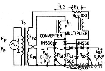
Multiplies d-c voltages ES1 and ES2 in two-stage arrangement in which converter is input stage con trolled by one signal voltage and multiplier is output stage controlled by other signal voltage.-J. Markus, Handbook of Electronic Control Circuits, McGraw-Hill, N.Y., 1959, p 103. (View)
View full Circuit Diagram | Comments | Reading(714)
SPACECRAFT_COMPUTER_POWER_SWITCHING
Published:2009/7/12 21:49:00 Author:May

Conserves battlery power by automatically disconnecting sections of computer when they are nol in use. Q1 and Q2 serve as switch,while Q3 generates automatic reset pulse when power turns on.When control line is at ground,no power is supplied on output line.Q4 delays Power turnoff for short time after control signal drops.-R.A.Clift,Power Switching Trims Digital System Weight, Cost Electronics,39:12,p135-138. (View)
View full Circuit Diagram | Comments | Reading(811)
FET_CONVERTS_TRIANGULAR_TO_SINE
Published:2009/7/17 1:43:00 Author:Jessie

Eliminates need for signal rectification by using symmetrical properties of Fairchild FSB40 fet with respect to source and drain. For p-channel units, reverse the diodes.-R. D. Middlebrook and 1. Richer, Nonreactive Filter Converts Triangular Waves to Sines Electronits, 38:5, p 96-101. (View)
View full Circuit Diagram | Comments | Reading(750)
LOW_RFI_AC_LIMITER
Published:2009/7/17 1:42:00 Author:Jessie


This current limiter will work with any ac device. It does not need a zero-crossing network be-cause it is not based on a triac. Instead, a current-limiting circuit reduces the peaks of the ac waveforms. That is preferable to the action of a triac in a light dimmer, which suddenly turns on and generates significant RE harmonics (even with a zero-crossing network) in all but the fully ON state. (View)
View full Circuit Diagram | Comments | Reading(3658)
FLASH_EEPROM_COMMUNICATOR
Published:2009/7/12 21:49:00 Author:May
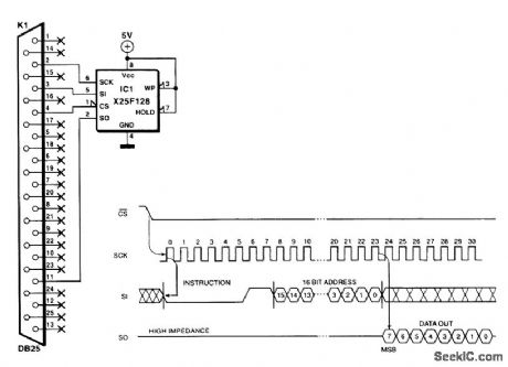
Modern equipment frequently uses serial EEPROMS to store data that must not be lost. With the circuit shown, it is possible to program or read such an IC via the Centronics port of a computer. Because the serial interface of a flash EEPROM is identical to that of an EEPROM, the two devices can communicate with each other. This means that the present circuit can be used for either device. The IC is enabled via CS (Chip Select). The command read followed by the address that needs to be read is set on to the high level is a little low, some 4.7 kΩ pull-up resistors can be added between the Centronics outputs and the positive supply line (not the SO line). (View)
View full Circuit Diagram | Comments | Reading(1190)
_5_V_AT_425_mA_
Published:2009/7/17 1:42:00 Author:Jessie

Developed for syllabic VOX system used with Drake T-4XB and R-4B transmitter and receiver. Input is taken from 12.6-VAC transformer winding of power supply for Drake, so equipment power switch also turns off 5-V supply. - R.W. Hitchcock, Syllabic VOX System for Drake Equipment, Ham Radio, Aug. 1976, p 24-29. (View)
View full Circuit Diagram | Comments | Reading(668)
DOUBLE_BRIDGE_OPEN_FUSE_DETECTOR
Published:2009/7/17 1:42:00 Author:Jessie

Used with magnetic amplifier to disconnect d-c voltage from section protected by fuse that opens. Output of lower bridge is balanced against output of upper bridge by adjusting R1. Gives greatly increased sensitivity.-J. Maroz, Magnetic Amplifier Detects Open Fuses, Electronics, 31:29, p 86-92. (View)
View full Circuit Diagram | Comments | Reading(612)
TWO_SPEED_SERVO_MOTOR_DRIVE
Published:2009/7/17 1:41:00 Author:Jessie
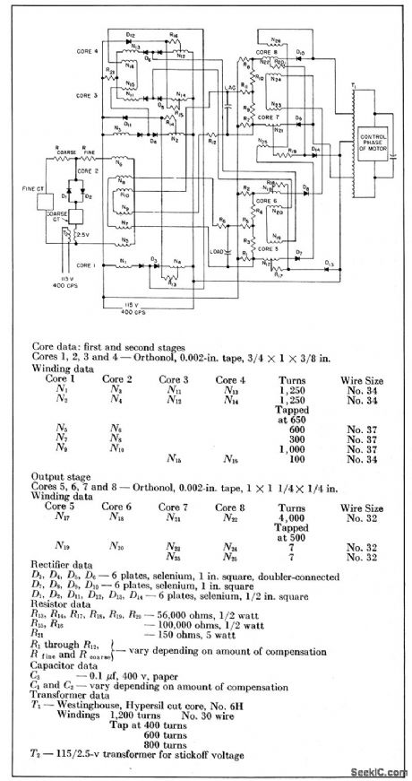
Consists of two conventional half-wave bridge-type stages driving full-wave slave-type output stage. Designed to replete former electron-tube amplifier of two-phase servo system using fine and coarse control transformers.-J. Markus, Handbook of Electronic Control Circuits, McGraw-Hill, N.Y., 1959, p 112. (View)
View full Circuit Diagram | Comments | Reading(631)
SERIAL_TRANSMITTER_CIRCUIT
Published:2009/7/12 21:48:00 Author:May

This circuit provides basic parallel-to-serial conversion, with the control inputs connected to provide a word format of 1 start bit, 8 data bits, 1 stop bit, and no parity. VR1 should provide operation at 1200 baud. Adjusting VR1 is just a matter of using trial and error to locate a setting that enables the computer to reliably decode the serial data. If a frequency meter is available, adjust VR1 for an output frequency of 19.2 kHz at pin 3 of IC2. (View)
View full Circuit Diagram | Comments | Reading(2446)
INEXPENSIVE_EMERGENCY_LIGHT
Published:2009/7/17 1:41:00 Author:Jessie

This low-cost circuit charges two nickel-cadmium cells to provide a standby power supply for a two-lamp emergency light, which is automatically switched on in the event of a power failure. Diode D1 and smoothing capacitor C1 form a conventional single-phase rectifier circuit with an output voltage of about 6 V. This voltage is used to continuously charge two series-connected NiCd batteries with a current of 80 to 100 mA, which flows via R1 and D2. At this rate, a 2-Ah (ampere-hour) NiCd battery can be safely charged for extensive periods. The voltage drop across D2 reverse-biases the base-emitter junction of PNP transistor T1. Consequently, the transistor is turned off, and the lamps connected, to its collector do not light. When a power outage occurs, T1 is supplied with base current (from the batteries) via R2, whereupon the miniature lamps are turndd on. As soon as the power is restored, T1 is switched off again, and the batteries are charged again via RI and D2. (View)
View full Circuit Diagram | Comments | Reading(3147)
40_W_RAPID_START_BALLAST
Published:2009/7/12 21:47:00 Author:May

AC line volage is rectified by diode bridge andfiltered by biode bridge and filtered by C6-L1ATransistorsQ1-Q2 with center-tapped tank coil T1A and C1- C3 make up ρower stage of 20-kHz oscillator that develops 600 V P sine wave across T1A. When fluorescent lamps ionize, current to each is limited to about 0.4 A. Lamps operate independently, so one stays on when other is removed Feedback transformer T2A supplies base drive for transistors and filamentpower forlamps Article gives transformer and choke winding data.-R J Haver,The Verdict Is In:Solid-State Fluoresce Ballasts Are Here,EDN Magazine, Nov,5,1976,p 65-69. (View)
View full Circuit Diagram | Comments | Reading(1320)
JOYSTICK_CHANGEOVER
Published:2009/7/12 21:46:00 Author:May

Many I/O cards and sound cards have a standard provision of a 15-way connection for two joysticks. Unfortunately, many programs use the connections for only one joystick. Because often several kinds of joystick are used (in particular, modern flight simulators have provision for very advanced, specialized joysticks), it is frequently necessary to change over connectors. As the joystick connectors are invariably found at the back of the computer, this can be a tedious operation.Moreover, in the long term, it does not do the connectors any good. The present circuit replaces this changing over of connectors by a simple push on a button. In this way, two joysticks can be connected to the computer in a simple and user-friendly way. An eight-pole switch arranges the interconnection of controls X and Y and fire button 1 and fire button 2. (View)
View full Circuit Diagram | Comments | Reading(587)
COMPUTER_VOICE
Published:2009/7/12 21:45:00 Author:May

This circuit will enable one to simulate the computer voice effect commonly heard in films, ads, and TV programs. It consists of two sections: an oscillator to provide the modulation signals, and the modulator itself. The oscillator uses a 555 timer chip in the astable multivibrator mode, and the frequency of operation has been set at about 10 Hz by the values given to R1, R2, and C1. A very simple modulator is used, but this is quite acceptable. Distortion produces new frequencies that help to change the voice signal and make it sound less like the original. A large amount of distortion is obviously not desirable because it would severely impair the intelligibility of the output signal. Transistor TR1 is used as a sort of voltage-controlled resistor, and, in conjunction with R4, it forms a voltage-controUed attenuator. (View)
View full Circuit Diagram | Comments | Reading(2031)
VOLTAGE_COMPARATORS
Published:2009/7/12 21:44:00 Author:May

These two comparators are over- and under-voltage comparators. In Fig. 104,5(a), if VIN exceeds the reference voltage, the output of IC1 goes low. In Fig. 104-5(b). if the VIN exceeds the reference, VOUT goes high. (View)
View full Circuit Diagram | Comments | Reading(666)
PC_POWER_PINCHER
Published:2009/7/12 21:43:00 Author:May

The figure is a diagram of the circuit, in which a low-frequency oscillator continually drives the input of a multistage binary counter. Whenever the count reaches the setting selected by DIP switch S1, the circuit turns triac Q3 off, thereby interrupting the flow of 120-Vac to the monitor. A keyboard-monitoring circuit keeps the video monitor powered up during active use by resetting the counter every time a key is pressed. As long as a keypress occurs before the time delay expires, the counter keeps resetting. Hence, it never times out, and the monitor continues to receive power. When the computer turns on, a routing in its basic input/output system (BIOS) polls the keyboard. The keyboard, in turn, sends a series of data pulses back to the microprocessor to indicate its status. The data line is normally high (+5 V), and the pulses are low-going transitions. The first stage of the power pincher inverts the sense of the logic to normally low with high-going transitions. (View)
View full Circuit Diagram | Comments | Reading(1103)
MINIMUM_DRAIN_TIMER
Published:2009/7/12 21:42:00 Author:May
National LM122 timer is connected to reduce supply drain to zero between timing cycles. External PNP transistor Q1 serves as latch between V+ ternlinal of timer and power supply. Between timing periods, Q1 is off and no current is drawn. Arrival of 5-V or larger trigger pulse turns Q1 on forduration of timing period set by Rt and Ct, which can range from microseconds to hours. -C. Nelson, Versatile Timer Operates from Microseconds to Hours, National Semiconductor, Santa Clara, CA, 1973, AN-97, p 10. (View)
View full Circuit Diagram | Comments | Reading(697)
DISK_READ_WRITE
Published:2009/7/12 21:41:00 Author:May

Magnetic head is transformer of twin-triode blocking oscillator circuit used with aluminum disk having radial magnetic spokes that can store from 50 to 100 words.-T. C. Chen and O. B. Stram, Digital Memory System Keeps Circuits Simple, Electronics, 32:11, p130-133. (View)
View full Circuit Diagram | Comments | Reading(585)
WINDOW_DETECTOR
Published:2009/7/12 21:41:00 Author:May

The high switching speed, low offset current and low offset voltage of the HA-4900 series make this window detector extremely well-suited for applications that require fast, accurate decision-making. This circuit is ideal for industrial-process system-feedback controllers, or out-of-limit alarm indicators. (View)
View full Circuit Diagram | Comments | Reading(0)
| Pages:760/2234 At 20741742743744745746747748749750751752753754755756757758759760Under 20 |
Circuit Categories
power supply circuit
Amplifier Circuit
Basic Circuit
LED and Light Circuit
Sensor Circuit
Signal Processing
Electrical Equipment Circuit
Control Circuit
Remote Control Circuit
A/D-D/A Converter Circuit
Audio Circuit
Measuring and Test Circuit
Communication Circuit
Computer-Related Circuit
555 Circuit
Automotive Circuit
Repairing Circuit