
Circuit Diagram
Index 744
Ear Drop Amplification Circuit
Published:2011/7/17 23:32:00 Author:Felicity | Keyword: Ear Drop, Amplification Circuit
View full Circuit Diagram | Comments | Reading(590)
±15_V_FOR_SOUND_SYNTHESIZER
Published:2009/7/16 22:28:00 Author:Jessie

Provides highly stabilized voltages, required by elaborate sound synthesizer developed for generating wide variety of musical and other sounds. Circuit has additional 5-V output Tr6 requires heatsink dissipating 0.6 W, while heatsinks for Tr5 and Tr7 must each dissipate 14 W. Bridge rectifier is rated 100 V inverse peak at 2 A. Three-part article gives all circuits used in synthesizer.-T. Orr and D. W. Thomas, Electronic Sound Synthesizer, Wireless World, Part 3-Oct. 1973, p 485-490 (Part 1-Aug. 1973, p 366-372; Part 2 Sept.1973, p 429-434). (View)
View full Circuit Diagram | Comments | Reading(807)
SWITCHABLE_LINEAR_VOLTAGE_REGULATOR
Published:2009/7/16 22:27:00 Author:Jessie

This three-voltage regulated supply can be added to for more voltage ranges. (View)
View full Circuit Diagram | Comments | Reading(689)
17_W_5_V_AND_33_V_POWER_SUPPLY
Published:2009/7/16 22:27:00 Author:Jessie

The low concerns of today's notebook computer designs do not have to restrict designers to low-performance solutions. The logic power supply is usually required to furnish excellent regulation at extremely high efficiency, but also carry a small price tag. This LTC1149 circuit addresses these requirements by using a single synchronous rectifier controller IC to generate both 3.3- and 5-V logic supplies. The 3.3-V output is generated in normal step-down regulator fashion using synchronous switches and an inductor. The key to circuit operation is the extra winding on the inductor and its corresponding synchronous rectifier, QN2. These provide the 5-V output by using transformer action. Cross regulation with this circuit is excellent because of the use of a trifilarwound inductor and a split feedback, which combines both outputs into the same feedback net-work. Efficiency exceeds 90 percent over most of the operating range. In addition, the 3.3- and 5-V outputs are inherently synchronous in switching frequency, and they will reach their rated voltage at the same time after power-up. Another bonus is that is if one logic supply is short-circuited, the other output will be disabled. (View)
View full Circuit Diagram | Comments | Reading(663)
_5_V_AND_±6_OR_±12V
Published:2009/7/16 22:24:00 Author:Jessie

Three power supplies for experimental use are achieved with only one transformer. LM309K regulates 5-V supply. Other two supplies are regulated by 6.2-V zeners in conventional regulator; shorting out one zener in each with gang switch reduces output to 6 V.- Design a Circuit Designer!, 73 Magazine, Oct. 1977, p 152-153. (View)
View full Circuit Diagram | Comments | Reading(727)
HANDY_HOBBY_POWER_SUPPLY
Published:2009/7/16 22:24:00 Author:Jessie

The input voltage to the power supply at mini phono jack J1 must be from 7 to 20 Vac or from 7 to 30 Vdc. You can use any transformer or ac-to-dc wall adapter that meets those input requirements. An ac input at J1 is rectified by bridge rectifier BR1; a dc input passes through half of the rectifier unmodified, except that its value drops by the sum of two diode voltage drops. Two MC7805 5-V regulators are in the circuit: IC1 provides a fixed 5-Vdc output at J2, while IC2 has a variable dc output at J3. The variable output ranges from +5 Vdc to 2 V less than the input voltage to the power supply. The output of the fixed regulator is made variable by varying the voltage at pin 2 with potentiometer R1. (Pin 2 is normally grounded to produce the fixed-voltage output.) Each voltage regulator can safely handle up to 1 A of current, provided that the transformer or power adapter can handle the demand and that the regulator is properly heatsinked. The voltage regulators must be heatsinked if more than a few milliamperes is to be drawn from the supply. Power indicator LED1 is connected across the fixed 5-V output; it lights whenever the supply is powered. (View)
View full Circuit Diagram | Comments | Reading(1649)
126_V_AT_3_A
Published:2009/7/16 22:23:00 Author:Jessie

Article gives step-by-step procedure for designing simplest possible regulated supply to meet specific requirements in general service. Power transformer rated 12.6 V at 3 A delivers about 18 V P to bridge rectifier rated 50 V at 5 A. Value of C1 is chosen to keep voltage to regulator above 15-V limit at which circuit would drop out of regulation.-C. W. Andreasen, Practical P. S. Design, 73 Magazine, June 1977, p 84-85. (View)
View full Circuit Diagram | Comments | Reading(735)
600_MICROSEC_OUTPUT_PULSE_MONO
Published:2009/7/16 22:23:00 Author:Jessie

Similar to fiip-flop except that one cross-coupling network permits a-c coupling only. Flip-flop can therefore remain in its unstable state only until reactive components discharge. Use of inductor in place of capacitor for timing gives much better pulse width stability at high temperatures. Operating range is -55 to 71 ℃.- Transistor Manual, Seventh Edition, General Electric Co., 1964, p 201. (View)
View full Circuit Diagram | Comments | Reading(633)
120_1_FREQUENCY_RANGE_ASTABLE
Published:2009/7/16 22:21:00 Author:Jessie

Modified astable has frequency change of 5 to 600 millisec at 50% duty cycle, with symmetry variable by 97.5%. Can be used as pattern source for generating keyed d-c or keyed tone signals for testing digital communications and data processing equipment.-Wide Range Variable Multivibrator, Electronic Circuit Design Handbook, Mactier Pub. Corp., N.Y., 1965, p 109. (View)
View full Circuit Diagram | Comments | Reading(657)
POWER_ON_CONTROL_WITH_POWER_ON_RESET
Published:2009/7/16 22:21:00 Author:Jessie

A power-management control device for high-power interfaces in battery-operated equipment can incorporate a power-on-reset (POR) function. The power control is provided by a P-channel MOSFET in a conventional switching configuration. The POR function is supplied by the DISCHARGE pin of a CMOS version of a 555 timer. The circuit holds the POR line low while power to the device interface is off. However, when the interface device is turned on, its power rises immediately, and a delay to release the P0R line is initiated. The threshold voltage on the 555 trigger comparator is about 1.7V. If the component values for R1, R2, and C1 are applied, the capacitor voltage decays to the threshold value in about 1.6 ms. When the capacitor voltage decays below the threshold value, the POR line is released. Diode D2 provides threshold hysteresis and raises the POR threshold voltage to approximately 2.5 V at the output-stale transition. (View)
View full Circuit Diagram | Comments | Reading(1394)
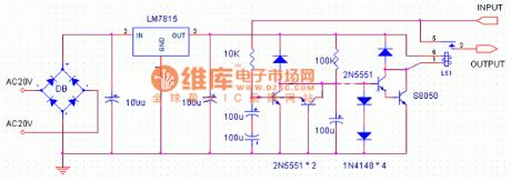
POWER_SUPPLY_FOR±12_V_AND±5_V
Published:2009/7/16 22:21:00 Author:Jessie

This supply is suitable for small projects that need up to 30 mA at ±12 V and 0.5 A at ±5 V. (View)
View full Circuit Diagram | Comments | Reading(731)
DUAL_POLARITY_LOW_CURRENT_POWER_SUPPLY
Published:2009/7/16 22:19:00 Author:Jessie

The 555 is operating in a free-running oscillator at about 120 kHz, producing a near-9-V square-wave output at pin 3. Diodes D1 and D2, along with capacitors C4 and C5, make up the rectifier circuit for the positive supply, while D3, D4, C2, and C3 make up the rectifier for the negative supply. (View)
View full Circuit Diagram | Comments | Reading(679)
INTERFACE_FOR_AC_LOAD_CONTROL
Published:2009/7/12 22:39:00 Author:May

Standard 7400 series gates provide input to Motorola MOC3011 optoisolators for control of triac handling resistive or inductive AC load. Gates are driven by MC6800-type peripheral interface adapters. If second input of two-input gate is tied to simple transistor timing circuit as shown, triac is energized only at zero crossings of AC line voltage. This extends life of incandescent lamps, reduces surge-current effect on triac, and reduces EMI generated by load switching.-P. O'Neil, Applications of the MOC3011 Triac Driver, Motorola, Phoenix, AZ, 1978, AN-780 p 6. (View)
View full Circuit Diagram | Comments | Reading(557)
TRANSIENT_IMMUNE_MONO
Published:2009/7/16 22:19:00 Author:Jessie

Diode in series with cutoff collector load of Q1 provides protection against undesirable triggering by power supply transients.-W. B. Smith, Jr., Transient-Protection of Monostable Multivibrators, EEE, 11:3, p 38-39. (View)
View full Circuit Diagram | Comments | Reading(671)
ANALOG_ELECTRONIC_LOCK
Published:2009/7/12 22:38:00 Author:May

The system is formed of two separate circuits-a key and a keyhole. The key engages the keyhole by means of a mating pair of connectors. The key is a tone-generator circuit consisting of a 4049 hex inverter CMOS IC (U1), switches (S1 and S2), a resistor (R1), and a capacitor (C1). The value of the tone generated by that circuit, in hertz, is determined by 1/(1.4XR1C1) The keyhole is a 567 tone-decoder circuit that can be configured to detect any frequency from 0.01 Hz to 500 kHz. The frequency it detects (fo)is set by resistor R2 and capacitor CZ, according to fo=1.1/(R2C2). When the key is inserted into the lock and switch S1 is pressed, a tone is supplied to the input of the keyhole circuit. If the tone frequency is close enough to fo, the 567IC turns on the relay (K1), which should be connected to the electronic locking device. Components R3 and D1 are used to latch the circuit, so that the output stays on even after the input tone is removed. When S2 is pressed, the system is reset. Switch S3 resets the circuit from inside. Note: The accuracy with which the keyhole circuit detects fo can be set by changing the values of three components. First, R2 should be between 2000 and 20,000 Ω . Second, the value in microfarads of capacitor C4 should be n/fo, where n is a value between 1300 and 0000 (which gives a detection accuracy of up to 14 percent of fo). Finally, capacitor C3 should have about twice the capacitance of capacitor C4. Battery B1 supplies both circuits.
(View)
View full Circuit Diagram | Comments | Reading(1195)
AUDIO_TO_DC_CONVERTER_CIRCUIT
Published:2009/7/12 22:38:00 Author:May

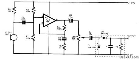
The circuit diagram for the audio input module, which produces a dc output voltage relative to the input signal amplitude. (View)
View full Circuit Diagram | Comments | Reading(1540)
75_kV_REGULATED_SUPPLY
Published:2009/7/12 22:38:00 Author:May

Power transformer is special design, but commercial unit delivering 5 to 10 kV can be used. Inverter circuit uses MJE105 transistor driving primaries of transformer. 741 opamp and transistor provide regulation for 7.5-kV output used in slow-scan TV monitor. Diodes are 1 kV, such as 1N4007.Article gives circuit of complete monitor, including low-voltage supply.-L.Pryor,Homebrew This SSTV Monitor, 73 Magazine, June 1975, p 22-24, 26-28, and 30. (View)
View full Circuit Diagram | Comments | Reading(1137)
8_BIT_BINARY_TO_DECIMAL_CONVERTER
Published:2009/7/12 22:37:00 Author:May
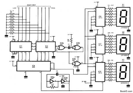
The decimal value of the eight input lines is displayed on three seven-segment displays. Although chips exist to perform this function for single displays, none include the possibility of displaying numbers greater than 9. No EPROM is necessary in this design. It operates by using two synchronized counters, one that generates an 8-bit binary output, and a second that drives the display. If the display is updated only when the binary counter is at the same value as the input, then the display will show the decimal value of the input. IC4 is the binary counter, and IC6 to IC8 form the display/counter section. IC5a and IC5b form the astable, which clocks both counters at 5 kHz.The minimum display refresh rate is, therefore, 20 times per second, IC1 and IC2 are two 4-bit comparators, ganged to form an 8-bit comparator. This compares the output of the binary counter (IC4) with the binary input taken from the circuit under test. Resistors RI to R8 pull down the input lines to prevent them from floating when no input is connected. When the comparator inputs are equal, pin 6 of IC2 goes high, triggering the monostable (IC3ab), which outputs a brief pulse. This latches the value of the display counters (IC6 to IC8) to the display. When IC4 reaches avalue of 256, the link between pins 11 and 12 resets the chip, and this resets the display counter also. (View)
View full Circuit Diagram | Comments | Reading(7981)
GYRATOR_CIRCUIT
Published:2009/7/16 22:18:00 Author:Jessie

The gyrator circuit has been around for a number of years. This active circuit can be used in place of an inductor. With two operational amplifiers (two sections of a dual or quad op amp are preferred), the value of the inductance simulated by this circuit is L=R1R2R3/(R2/R4) or, in the case where R2=R3, L=R1R5C4. (View)
View full Circuit Diagram | Comments | Reading(3100)
BENCH_POWER_SUPPLY
Published:2009/7/16 22:18:00 Author:Jessie

The ac voltage from transformer T1 is rectified by bridges BR1, BR2, and BR3 and filtered by capacitors C1, C2, C5, C6, and C9. Voltage regulators IC1 to IC5 reduce the voltage to the desired fixed or variable levels. The LM317 regulator, IC1, provides a positive variable output from 1.2 to 28 Vdc, and an LM337, IC2, provides a negative variable output with the same range. The LM7805 regulator, IC3, supplies a fixed +5 V, and the LM7905, IC4, supplies a fixed -5 V. The LM7812 regulator, IC5, supplies a fixed +12 V. Capacitors C3, C4, C7, C8, and C10 improve transient response and prevent oscillation. Resistor networks R1 through R3 and R2 through R4 for IC1 and IC2, respectively, provide the necessary feedback to obtain the variable output voltages. An LED and current-limiting resistor are wired across each output to indicate when each output voltage is present. The main power indicator for the entire unit consists of LED5 and R18. Switch S1 controls ac power to the transformer primary, and switches S2 and S3 connect the secondary voltages to the 5- and 12-V regulator circuits. The ±5-V supply powers the voltage meter And display circuitry, so this section must be turned on to power the output meter. Switch S4 is a two-pole, six-throw (2P6T) rotary unit. Pole A switches the positive input to the voltmeter and pole B switches the ground input.(Three separate grounds are in the circuit.) Pole A of S4 is connected to one pole of DPDT switch S5 so that the signal can be routed directly to the meter for voltage readings or to the LM741 current-to-voltage converter IC7 for current readings. The second pole of S5 is connected to the +5-V supply. This pole is switched to the second decimal point of the display in the Voltage mode or to pin 7 of the LM741 in the Current mode. (View)
View full Circuit Diagram | Comments | Reading(1127)
| Pages:744/2234 At 20741742743744745746747748749750751752753754755756757758759760Under 20 |
Circuit Categories
power supply circuit
Amplifier Circuit
Basic Circuit
LED and Light Circuit
Sensor Circuit
Signal Processing
Electrical Equipment Circuit
Control Circuit
Remote Control Circuit
A/D-D/A Converter Circuit
Audio Circuit
Measuring and Test Circuit
Communication Circuit
Computer-Related Circuit
555 Circuit
Automotive Circuit
Repairing Circuit