
Circuit Diagram
Index 742
10_dB_50_W_ATTENUATOR
Published:2009/7/12 22:54:00 Author:May
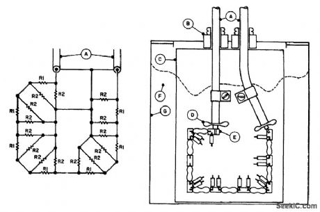
The 10-dB attenuator has an attenuation of 10 dB at lower frequencies at 2 m and 70 cm; circuit losses increase to 10.8 dB and 12.0 dB, including interconnecting RG-58/U cable losses of 0.4 dB and 0.6 dB, respectively. Establishing an SWR of less than 1.1:1 at 70 cm was the most crucial design consideration. Changes occur with different coolants. If the assembly is tailored for minimum SWR in air, its SWR increases to about 1.3:1 when you put it in vegetable oil. The SWR changes are caused by increased circuit capacitance due to the dielectric. This condition was improved by using household wax, paraffin, instead of oil. Cctution: Paraffin has ct relatively Lou;ftctsh temperature; it can be used to make candles. Next, to decrease the circuit distributed capacitance, increase the distance of the components from the circuit board by stacking two layers of PC boards at the tie-down pads.This raises the parts of connecting positions to about 0. 120 in. The completed assembly has an SWR of less than 1. 1 : 1 at both 70 cm and 2 m. Schematic and layout of the 10-dB attenuator: R1, 10-Ω 1/2-W (7); R2, 1-kΩ 1/4 W (14). A. Input/output, 3 ft RG-58/U. B. Cable bushing, 1/4 in. clearance hole. C. Component mounting board, 3 1/2 inX23/8 inX1/14, in PCB. D. Fan out end cable braid, twist into two segments, and solder to PCB with ntinimum lead lengths. E. Component tie-down pads (9), double thickness glass-epoxy PCB, 1/4inX1/8 inX1.8 in pieces cemented together and into position with clear household cement (Elmer's). F. Coolant, household wax (paraffin). Fill container with melted wax to 1/4 in from the top. To melt wax, insert the container in hot water (about 200°F). G. Container, one-pint can. (View)
View full Circuit Diagram | Comments | Reading(847)
ASTABLE_HYBRID_TD_TRANSISTOR_SQUARE_WAVE_GENERATOR
Published:2009/7/16 20:54:00 Author:Jessie

Fast switching capability of tunnel diode contributes to clean output waveform of mvbr configuration.- Trcmsistor Manual, Sevenlh Edition, General Electric Co.,1964, p 367. (View)
View full Circuit Diagram | Comments | Reading(642)
ISOLATED_15_V_TO_2_500_V_SUPPLY
Published:2009/7/16 20:54:00 Author:Jessie

A dc-dc converter using a 74HC04 drives T1. T1 is a ferrite-core transformer using a Fair-Rite, Inc. P/N 5975000201 (μo + 5 000) and has a 7-turn primary and a 25-tum secondary. Kynar, #30 wirewrap wire is used. With T1, the circuit isolation is good to 2 500 V. (View)
View full Circuit Diagram | Comments | Reading(739)
VOLTAGE_CONVERTER
Published:2009/7/12 22:52:00 Author:May
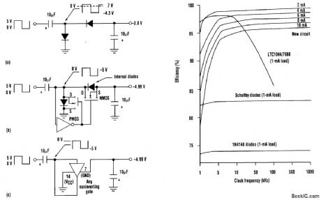
This bootstrap voltage converter begins with the basic diode inverter circuit (a). Placing a MOSFET across each diode will improve efficiency (b). The final step involves using a single noninverting CMOS digital gate to replace the diodes (c).The performance curves depict the bootstrap voltage converter's efficiency, which is 99 percent from 5 to 500 kHz using 10-μF capacitors and a 1-mA load. A typical commercial unit operates at only 94 percent efficiency. (View)
View full Circuit Diagram | Comments | Reading(1042)
INDUCTORLESS_BIPOLAR_SUPPLY_GENERATOR
Published:2009/7/16 20:54:00 Author:Jessie

Localized generation of bipolar supply rails is useful in many op-amp, data-conversion, and interface applications. To avoid the design time and effort of putting together a switching regulator circuit, switched-capacitor conversion should be considered as a simple, effective alternative. The LT1026 is shown here in a useful application circuit that can generate rail voltages of both polarities from a 5-V logic supply. Output voltage will vary with load (as shown on the graph), from ±9 V at minimal load currents to ±6 V at a load current of 15 mA. These boosted rails can be used to extend comrnon-mode input and output ranges of circuits without doing level shifting, ac coupling, or signal clipping. Because the LT1026 is supplied in an eight-lead SO package, the entire circuit can be surface-mounted using tantalum or ceramic capacitors. (View)
View full Circuit Diagram | Comments | Reading(817)
AUTOMATIC_VOLTAGE_CONTROLLER
Published:2009/7/12 22:51:00 Author:May

Station dc voltage, a nominal 113.8 Vdc, is fed through the normally closed contacts of relay K2. This voltage also provides power for the protective circuit illustrated. The voltage appears across R1 and R2, 10-kΩ trimpots, the wipers of which are set to exactly midrange, measuring a nominal 16.9 V dc. As the station dc varies between 111.2 and 115 V, the voltage at the wipers will vary from 5.6 to 7.5 Vdc. Zener diode D2 controls the high-voltage limit of 115 Vdc. R5 and zener diode D4 control the low-volt-age limit of 111.2 Vdc. Avoltage is fed from the wiper of R1 directly to the base of Q1, relay K1 is not energized, and its normally open contacts prevent relay K2 from being energized, allowing station dc to flow through K2's normally closed contacts. Above 115 V, the voltage at the base of Q1 also rises to or above 17.5 V, energizing K1, whose normally open contacts close, energizing K2, whose normally closed contacts open, removing the voltage from the station equipment. Should the voltage fall to or below 111.2 Vdc, zener diode D4 ceases to conduct, cutting off Q2, which causes Q3 to conduct, energizing K3. K3 applies operation voltage through its contacts to the coil of relay K2, opening its normally closed contacts, removing voltage from D6, the station equipment, and applying power to LED D7 and the audible alert.
(View)
View full Circuit Diagram | Comments | Reading(764)
VOLTAGE_CALIBRATOR
Published:2009/7/16 20:54:00 Author:Jessie

A NE555 oscillator drives a regulator to provide a regulated square-wave voltage to a voltage divider. The output is 1 to 5V p-p in 1-V steps. (View)
View full Circuit Diagram | Comments | Reading(977)
D_C_TO_100_MC_DEFLECTION_AMPLIFIER
Published:2009/7/16 20:53:00 Author:Jessie

Gain is constant within 3 db of 40 db over entire 100-Mc bandwidth, for driving electrostatic deflection plates of oscilloscope.-L.L.Kossakowski,Designing a D-C to 100-MC Deflection Amplifier, Electronics, 35:17, p 64-66. (View)
View full Circuit Diagram | Comments | Reading(704)
INVERTER_OUTPUT_STAGE_OF_A_DC_TO_DC_CONVERTER
Published:2009/7/16 20:53:00 Author:Jessie

This figure shows the circuit diagram for an inverter output stage. (View)
View full Circuit Diagram | Comments | Reading(578)
MOBILE_±_35_V_5_A_AUDIO_AMPLIFIER_SUPPLY
Published:2009/7/16 20:53:00 Author:Jessie
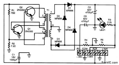

This ± 35-V supply uses a two-transistor multivibrator with a toroidal transformer. The transformer core is obtainable from Magnetics, Inc. Specifications for T1 are:
(View)
View full Circuit Diagram | Comments | Reading(982)
ISOLATED_3_V_TO_5_V_DAC
Published:2009/7/12 22:50:00 Author:May


The circuit uses a low-power (1 W) dc-to-dc converter for the power isolation and a transformer isolator/translator for the data interface. The transformer isolator not only provides the galvanic iso-lation required, but also converts the data signals between 3-V and 5-V levels. As a result, no additional level conversion is required. The ADC can run at 1-MHz clock rates. To allow the 50 percent duty cycles (clock and data signals) to pass through a transformer isolator requires an edge-detection and conversion technique. The edge detector is built from simple logic gates (two inverters and three NAND gates) and a short delay (either a delay line or a passive RC circuit can be used). The signal is rebuilt with a D-type flip-flop. Using a four-channel isolator allows full control over the ADC to be exercised. Conversion is requested by pulling the Chip Select pin low, and a Status high for one clock cycle is reported back to acknowledge conversion start. The first data bit (MSB) then is presented onto the data line, and all eight bits are transferred with a further Status signal at the end of conversion. Conversion can be requested asynchronously with the system clock, if necessary, and the Status flag can be used to poll the controlling logic circuitry. Filtering is placed on either side of the dc-to-dc converter to reduce power-supply ripple and prevent noise on the logic power supply from affecting the analog system. Although not shown, all ICs have 0.22-μF decoupling capacitors. (View)
View full Circuit Diagram | Comments | Reading(1040)
30s timing circuit formed by PUT
Published:2011/8/2 10:11:00 Author:Nancy | Keyword: 30s timing circuit, PUT
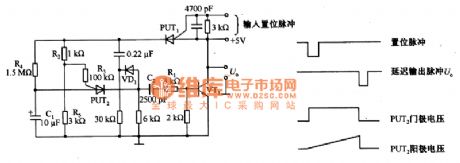
If you add a set pulse between the cathode-anode of PUT1, then PUT conducts, the + 5 V power supply charges C1 through it, the voltage of C1, which is the anode voltage of PUT2, increases gradually. When the anode voltage is higher than the gate bias voltage, PUT2 conducts, the discharging current of C1 flows through the drive transistor VT1 to make it saturate and conduct, the output Uo is close to OV. The C1 voltage add a reverse bias to PUT1, PUT1 cuts off to make the circuit reset. The output pulse width is basically decided by the C2 and R1, the pulse width is about 10 us. The delay time of the output pulse is decided by the R2, R3, R4 and C1. (View)
View full Circuit Diagram | Comments | Reading(553)
20_μA_QUIESCENT_CURRENT_REGULATOR
Published:2009/7/16 20:53:00 Author:Jessie

Knowing when the battery voltage is getting low allows equipment to arrange time to save valuable information. The LT1120A not only provides micropower, low-dropout regulation, but also includes a tow-battery detection comparator, all in an eight-lead DIP or SO package. The LT1120A supplies up to 125 mA at regulated voltages from 2.5 to 20 V. The low dropout voltage of 0.6 V (max.) lowers the battery input voltage requirements, and the small 40-μA (max.) quiescent current extends battery life. The LT1120A has yet more functions. The logic-compatible SHUTDOWN pin removes power to the load. The precision 2.5-V reference has the ability to both sink and source current to supply low-power backup circuits. Also, the LT1120A's design prevents excessive current draw when in dropout. (View)
View full Circuit Diagram | Comments | Reading(634)
MULTISWITCH_CHARGE_PUMP_BOOST_CONVERTER
Published:2009/7/12 22:47:00 Author:May
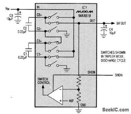
This device is useful both in main supplies and in backup supplies. It generates a regulated 5-V output for load currents to 20 mA and inputs ranging from 1.8 to 3.6 V. For input voltages no lower than 3 V, the output current can reach 50 mA. The circuit accomplishes regulation without a linear pass element, but its losses are the same as those of an unregulated doubler or tripler feeding into a linear regulator. (View)
View full Circuit Diagram | Comments | Reading(680)
100_W_SINE_AT_60_Hz
Published:2009/7/12 22:46:00 Author:May

Consists essentially of 60-Hz sine-wave oscillator with 10K frequency-control pot, two buffer stages, and push-pull power amplifier. Circuit eliminates noise problems of square-wave inverters when operating 115-V radio receiver or cassette player in car.- G. C. Ford, Power Inverter with Sine Wave Output, 73 Magazine, May 1973, p 29-32. (View)
View full Circuit Diagram | Comments | Reading(3501)
RATIOMETRIC_20_kHz_V_F_CONVERTER
Published:2009/7/12 22:46:00 Author:May

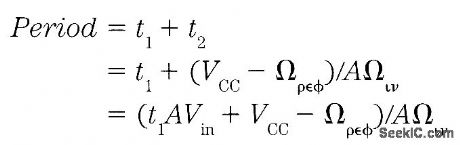

This ratiometric 20-kHz voltage-to-frequency converter (VFC) provides superior perforrnance with strain gauges and other ratio-responding transducers-even with noisy, unregulated excitation voltages. Feedback isn't used to achieve the excellent 4-Hz linearity, so there is very-low-frequency jitter-period measurements can be used to get several digits of resolution- even when operating at a fraction of full scale. An optional synchronizing transistor starts the VFC with zero charge at the beginning of each count cycle, eliminating the characteristic digit-jumping often encountered with VFC designs. Grood linearity is attained by making the comparator's reference voltage vary with the input voltage, which precisely compensates for the finite capacitor reset time:where AVin△V/△t. If Vref is made to include the amount t1AVin, then the effect of t1 is elirninated:The MPSA18 is a remarkably high-gain transistor, even at low currents, producing good current-source linearity down to 0 Hz. In addition, bipolar transistors work well with the low collector voltages encountered in this single-supply 10-V design. Moreover, most single-supply op amps will work in place of the LM10. But the LM10 also has a reference amplifier that could be used to construct a 10-V excitation regulator. The LM311 propagation delay gives a reset pulse width near 400 ns, which gives the transistor time to discharge the capacitor. Also, the 311's bias current produces a small negative offset that ensures a 0-Hz output for Vin. (View)
View full Circuit Diagram | Comments | Reading(800)
RAIN_ALARM
Published:2009/7/12 22:45:00 Author:May

This rain-detector circuit closes the relay when water bridges the gap between the metal elecLrodes. (View)
View full Circuit Diagram | Comments | Reading(0)
STOPWATCH
Published:2009/7/12 22:45:00 Author:May
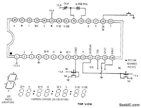
Intersil 7045 IC provides capability for driving digital display of time in hundredths of a second up through hours in four different operating modes selected by lower switches: sequential, standard, split, or rally. Grounding pin 9 momentarily with start switch initiates timing action. Repeated pressings of swhch activate operatirlg modes as selected. Grounding reset pin 16 clears stopwatch. IC can be connected directly to LED display, without drivers or resistors.-D. Lancaster, CMOS Cookbook, Howard W. Sams, Indianapolis, IN, 1977, p 159. (View)
View full Circuit Diagram | Comments | Reading(2346)
TAMPER_ALARM
Published:2009/7/12 22:44:00 Author:May

The silicon-controlled rectifier (SCR1) operates as a memory device to indicate a security breach in a room, desk drawer. safe. etc. Switch S1 can be a mechanical or magnetic switch. Position S1 in an object that you want to keep protected, making sure that the switch will close when the object is tampered with. When S1 closes, SCR1 turns on, lighting LED1. Pressing S2 resets the circuit. (View)
View full Circuit Diagram | Comments | Reading(943)
PORTABLE_CRO_TRIGGER_INPUI_AMPLIFIER
Published:2009/7/16 20:52:00 Author:Jessie
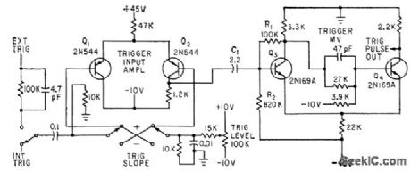
Schmitt trigger mvbr Q3-Q4 is modified by R1, R2, and C1 to give stable presentation at 2 Mc, with synchronization up to 4 Mc.-O. Svehaug and J. R.Kobbe,Battery Operated Transistor Oscilloscope, Electronics, 33:12, p 80-83. (View)
View full Circuit Diagram | Comments | Reading(673)
| Pages:742/2234 At 20741742743744745746747748749750751752753754755756757758759760Under 20 |
Circuit Categories
power supply circuit
Amplifier Circuit
Basic Circuit
LED and Light Circuit
Sensor Circuit
Signal Processing
Electrical Equipment Circuit
Control Circuit
Remote Control Circuit
A/D-D/A Converter Circuit
Audio Circuit
Measuring and Test Circuit
Communication Circuit
Computer-Related Circuit
555 Circuit
Automotive Circuit
Repairing Circuit