
Circuit Diagram
Index 740
PARALLEL_INVERTER_DRIVE
Published:2009/7/12 23:04:00 Author:May

Uses Mullard modules for converting DC power to AC at high power levels for such applications as driving induction motors at higher speeds than are obtainable with line frequency. DC control voltage of 0-10 V varies output frequency up to 400 Hz.UPA61 modules provide functions of level detector, pulse generator, ramp generator, capacitor discharge circuit, and bistable MVBR for parallel inverter system. RSA61 and TT61 are trigger modules, with RSA61 also providing power supplies for other modules.- Universal Circuit Modules for Thyristor Trigger Systems (61 Series), Mullard, London, 1978, Technical Information 66, TP1660, p 19. (View)
View full Circuit Diagram | Comments | Reading(973)
UP_DOWN_COUNTER_WITH_XOR_GATES
Published:2009/7/12 23:02:00 Author:May

This circuit shows how a regular 4-bit binary counter can be extended with an up/down function just by adding four XOR (exclusive-OR) gates. The principle is simple: The level at the common in-puts of the XOR gates determines whether the gates invert the counter's QA to QB output levels or not. In this way, the outputs of the XOR gates can be made to cycle from 1111 dowtt to 0000 instead of from 0000 to 1111. The disadvantage of this circuit over a real up/down counter is the jump, which occurs when the level on the U/D control input is changed. The sum of the old state and the new state is always 15. For example, if the counter is at state 3 in count-up mode, the state becomes 12 when the U/D line is made logic high to initiate down counting. (View)
View full Circuit Diagram | Comments | Reading(1860)
2_m_HT_BASE_STATION_ADAPTER
Published:2009/7/12 23:02:00 Author:May

This device mates with a small handie-talkie (HT) and provides power and speaker interface as well as charging capability. It was designed for an Icom 02-AT, but can be adapted for other HTs as well.
(View)
View full Circuit Diagram | Comments | Reading(1159)
SIMPLE_FREQUENCY_DOUBLER
Published:2009/7/12 23:02:00 Author:May

This circuit uses only a single exclusive-OR gate and a couple of passive components. The width of the output pulses is determined by the time constant of the RC network,and the maximum input frequency cannot exceed 1/2RC. (View)
View full Circuit Diagram | Comments | Reading(4903)
VOLTAGE_CONTROLLED_PRR
Published:2009/7/16 21:05:00 Author:Jessie

Input change of only 0.5 v will change pulse repetition rate of generator by factor of more than 1 to 10,000,000. Output pulse is about 0.3 microsec wide, with rise and fall limes of 20 nsec. Addition of back-biased diode CR2 extends low-frequency limit below 0.05 pps.-G. Richwell, Wide-Range Voltage-Controlled Pulse Generator, EEE, 13:10, p 72-77.
(View)
View full Circuit Diagram | Comments | Reading(767)
POWER_SUPPLY_MONITOR
Published:2009/7/16 21:05:00 Author:Jessie

The power supply is monitored by T1, a low-voltage step-down transformer. A standard full-wave power supply is used on the secondary winding to illuminate LED D5, and also operate the relay RLA1 and charge a large-value electrolytic capacitor (C2). The relay has normally closed (NC) contacts, which remain open while mains power is present through transformer T1, allowing the output from the bridge rectifier to power the relay coil. Power failure causes the relay to drop out and the normally closed contacts will now connect the piezo buzzer across capacitor C2. The stored voltage across C2 is enough to sound the buzzer for several minutes. The relay contacts could alter-natively be used to drive an isolated circuit, such as a buzzer and battery. The circuit might also appeal to tropical fish keepers or possibly deep-freeze owners. (View)
View full Circuit Diagram | Comments | Reading(0)
ADJUSTABLE_SWITCHED_REGIJLATOR
Published:2009/7/16 21:04:00 Author:Jessie

Circuit shows method of using LM109, 7805, or other IC voltage regulator to provide output voltage that is higher than rated output of IC. Voltage pedestal is developed across R2 and R3 for adding to normal regulated output of IC. R4 adjusts amount of added voltage. Divider R1-R2 provides positive feedback into pedestal circuit of regulator, to allow switching of IC and transistor.-V. R. Krause, Adjustable Voltage-Switching Regulator, Wireless World, May 1976, p 80. (View)
View full Circuit Diagram | Comments | Reading(3342)
FOUR_MODE_FREQUENCY_COUNTER
Published:2009/7/12 23:01:00 Author:May
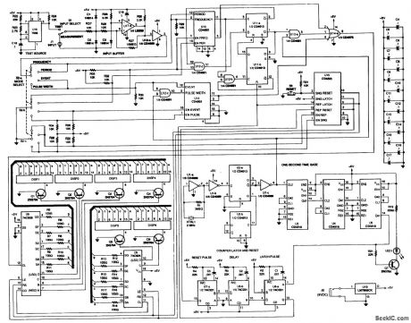
This counter can measure frequencies from 2 Hz to 1 MHz, time interval, and period, and count random events. A 74C926 and 74C925 are used as the counter, and these will drive a multiplexed LED display. A 2-MHz time base is used, and a divider chain is used to derive a 1-s gate. An LM339 op amp serves as the input buffer, and CD4000 series logic is used for gating and switching functions. (View)
View full Circuit Diagram | Comments | Reading(3296)
STROBE_POWER_SUPPLY
Published:2009/7/16 21:04:00 Author:Jessie

This 330-V power supply is a simple voltage doubler which provides 330 Vdc for a strobe circuit. This supply is not isolated from the power lines and extreme caution is advised. (View)
View full Circuit Diagram | Comments | Reading(811)
10_W_CW_TRANSCEIVER
Published:2009/7/12 22:59:00 Author:May
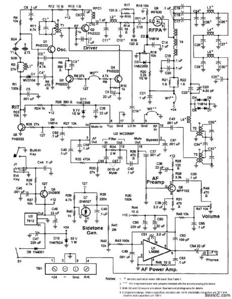
This transceiver can ioe operated on the 80-. 40-. or 30-m CW ham bands. A crystal oscillator drives a driver and RE PA delivering about 10 W output. The receiver uses an MC3359 IC and is fed LO from the crystal oscillator used for transmitting, and a varactor diode is used for incremental tuning (RIT) of the receiver. The unit also has a CW sidetone generator for ease of monitoring the transmitted CW signal. The power supply is 18 to 28 Vdc at 1 A. (View)
View full Circuit Diagram | Comments | Reading(3056)
ALIGNMENT_CORRECTION
Published:2009/7/16 21:04:00 Author:Jessie

Circuit developed for correcting alignment inaccuracies between electrostatic deflection plates and face of cathode-ray tube gives output varying from 0 to +3.5 V when input varies from 0 to-4 v.-F.E. Smith, Buffer Amplifier Supplies Bipolar Output,Electronics, 37:21, p 75. (View)
View full Circuit Diagram | Comments | Reading(813)
GaAsFET_BIAS_SUPPLY
Published:2009/7/16 21:03:00 Author:Jessie

Cellular telephones and other mobile communications gear use depletion-mode GaAsFET RE output transistors, which require a negative bias voltage for proper operation. This LTC1261 circuit generates a regulated negative voltage using no inductors, and will give plenty of drive for GaAsFET bias circuits. The LTC1261CS8 inverts the supply voltage (5 V to -4.5 V), whereas the LTC1261CS can invert or double the supply voltage (3 V to -4 or -5 V). Both parts regulate the generated output voltage. The quiescent current is just 600 μA, and the shutdown current is only 5 μA. The combination of high oscillator frequency, which reduces the switched capacitor size, and the variety of fixed-output regulated negative voltages allows for a minimum-space power supply. The LTC1261 comparator output controls a P-channel MOSFET to ensure that the drain current for the GaAsFET is switched off until the regulated negative output voltage is valid. This ensures that the gate voltage is sufficient to keep the GaAsFET off during power-up, preventing unsaturated operation and excessive operation. (View)
View full Circuit Diagram | Comments | Reading(939)
005_cps_TO_10_KC_POSITIVE_PULSES
Published:2009/7/16 21:03:00 Author:Jessie

Uses two -transistor equivalent circuit for double-base diode, to give better relictbility and more uniform performance in recycling timers, indicator readouts, and switching regulators. With parameter values shown, frequency is about 1 cps and pulse width is 30 millisec.-G. B. Mahoney, Low-Frequency Pulse Generator, EEE, 12:6, p 63-64. (View)
View full Circuit Diagram | Comments | Reading(769)
HIGH_VOLTAGE_GENERATOR
Published:2009/7/16 21:03:00 Author:Jessie

A 4049 Hex inverter drives an IRF731 hex FET. The 4049 is configured as an oscillator. Q1 should be heatsinked. T1 is an auto ignition coil. (View)
View full Circuit Diagram | Comments | Reading(3439)
CHARGE_PUMP_BOOST_CONVERTER
Published:2009/7/16 21:03:00 Author:Jessie

The circuit overcomes the charge pump's lack of regulation by adding a regulator externally. Another option-if load currents are modest-is to add regulation on the chip. Regulation in a monolithic chip is generally accomplished either as linear regulation or as charge-pump modulation. Linear regulation offers lower output noise; therefore, provides better performance in (for example) a GaAsFET-bias circuit for RF amplifiers. Charge-pump modulation (which controls the switch resistance) offers more output current for a given die size (or cost) because the IC need not include a series pass transistor. (View)
View full Circuit Diagram | Comments | Reading(905)
12_16_V_FROM_63_VAC
Published:2009/7/16 21:02:00 Author:Jessie

Designed for use with transistor or IC amplifier being fed by tube-type preamp having 6.3-V power transformer winding for filament supply. - K. D. James; Balanced Output Amplifier, Wireless World, Dec.1975, p 576. (View)
View full Circuit Diagram | Comments | Reading(763)
05333_136_s_WITH_LINE_FREOUENCY_ACCU_RACY
Published:2009/7/12 22:57:00 Author:May

Provides time delays in selected increments of 0.5333 s with accuracy essentially that of AClinefrequency. IC1 develops 120pulses per second having 100-μs width at pins 4 and 6 for each zero crossing of line. First six stages of IC2 determine basic timing period 1T, These stages produce pulse train with periodicity of 0.5333 s at input of seventh counter stage. Binary-or-dered output signals are available at outputs ah for 1T, 2T, 4T,.. 1287. Thus, for delay of 1 min (about 1127), use 64T + 32T, + 16T with AND-gate programming interconnections e-E, f-F, and g-G. Tie all unused AND-gate inputs to VDD bus.-A. C. N. Sheng, Line-Operated Timer Couples High Apeuracies with Long Time Delays, EDN Magazine, Jan. 5, 1976, p 37-40. (View)
View full Circuit Diagram | Comments | Reading(984)
HORIZONTAL_DRIVE
Published:2009/7/16 21:02:00 Author:Jessie

Three field-effect transistors give 45 db voltage gain for 1-cps riangular wave in horizontal defection circuit of crt.-F. J. Murphree and J. H. Hammond Jr., High-gain D.C Amplifier Drives CRT Display, Electronics, 37:19, p 53. (View)
View full Circuit Diagram | Comments | Reading(1114)
BASIC_STEP_UP_OUTPUT_STAGE_OF_A_DC_TO_DC_CONVERTER
Published:2009/7/16 21:02:00 Author:Jessie

This figure shows the basic circuit configuration for a step-up output stage. (View)
View full Circuit Diagram | Comments | Reading(722)
DIGITAL_COUNTER_CIRCUIT
Published:2009/7/12 22:56:00 Author:May

This circuit shows how a simple digital counter can be implemented. A CD4029B drives a DC4511 decoder and LED driver. A common-cathode LED display is used. (View)
View full Circuit Diagram | Comments | Reading(3092)
| Pages:740/2234 At 20721722723724725726727728729730731732733734735736737738739740Under 20 |
Circuit Categories
power supply circuit
Amplifier Circuit
Basic Circuit
LED and Light Circuit
Sensor Circuit
Signal Processing
Electrical Equipment Circuit
Control Circuit
Remote Control Circuit
A/D-D/A Converter Circuit
Audio Circuit
Measuring and Test Circuit
Communication Circuit
Computer-Related Circuit
555 Circuit
Automotive Circuit
Repairing Circuit